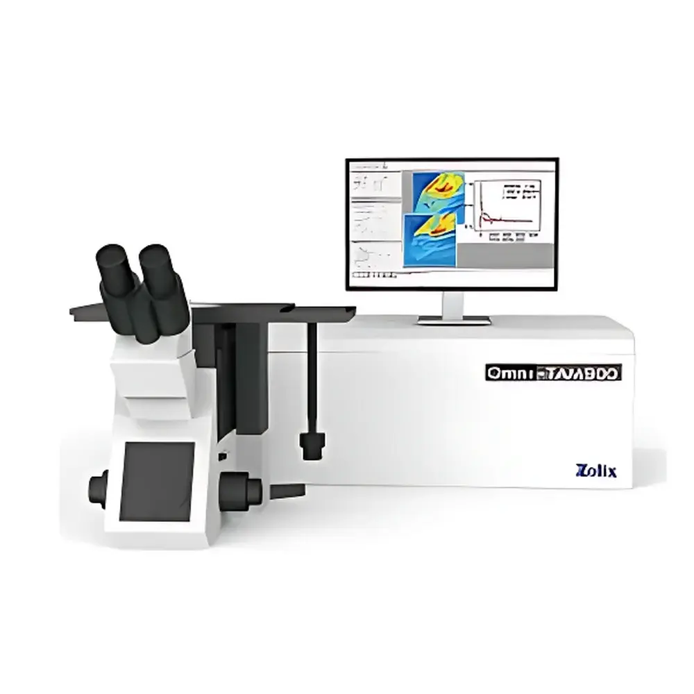
ZOLIX Omni-TAM900 Wide-Field Femtosecond Transient Absorption Imaging System
| Brand | ZOLIX |
|---|---|
| Origin | Beijing, China |
| Manufacturer Type | Original Equipment Manufacturer (OEM) |
| Product Category | Laser Flash Photolysis Instrument |
| Spectral Range | Application-Dependent (UV–NIR, configurable via OPA) |
| Spectral Resolution | <5 nm (typical, OPA-tunable) |
| Temporal Resolution | 500 fs (with 100-fs pump pulse) |
| Spatial Resolution | 500 nm |
| Carrier Localization Accuracy | 30 nm |
| Optical Delay Range | 0–4 ns / 0–8 ns (motorized precision delay line) |
| Detection | sCMOS camera with >95% quantum efficiency at 500–900 nm |
| Microscopy Platform | Inverted microscope with open-top design for cryostat, electrical biasing, magnetic field, and probe station integration |
| Operating Modes | Point Pump / Wide-Field Probe |
| Sample Illumination | Reflectance & Scattering Configurations Supported |
| Compliance | GLP-compliant data acquisition architecture |
Overview
The ZOLIX Omni-TAM900 Wide-Field Femtosecond Transient Absorption Imaging System is an integrated ultrafast optical platform engineered for spatiotemporal mapping of photoexcited carriers, excitons, and energy transfer processes at nanoscale spatial resolution and sub-picosecond temporal fidelity. Based on the pump-probe spectroscopic principle, the system combines femtosecond laser excitation (via Ti:sapphire oscillator + optical parametric amplifier), high-numerical-aperture inverted microscopy, and single-shot sCMOS imaging to capture transient absorption (ΔA) dynamics across both time and space domains simultaneously. Unlike conventional point-scanning transient absorption microscopes—limited by serial acquisition speed and signal-to-noise constraints—the Omni-TAM900 implements wide-field detection architecture, enabling parallel pixel-wise kinetic analysis over a 1024 × 1024 field-of-view without mechanical scanning. Its core innovation lies in proprietary interferometric signal amplification, which enhances weak ΔA contrast (as low as 10−5 ΔA/A) while maintaining quantitative linearity across four orders of magnitude in differential absorbance.
Key Features
- Two operational modalities: (1) Point-pump / wide-field probe mode for carrier migration velocity mapping and thermal diffusion coefficient extraction; (2) Wide-field pump / wide-field probe mode for spatially resolved carrier density distribution, heterogeneity analysis, and edge-state dynamics quantification.
- Sub-500 nm optical spatial resolution (diffraction-limited, λ = 532 nm excitation), with carrier localization accuracy down to 30 nm via centroid fitting of transient signal centroids.
- Temporal resolution of 500 fs, achieved using a motorized optical delay line with <10 fs RMS jitter and programmable step resolution of 0.5 fs over 0–8 ns range.
- Inverted microscope base with modular open-top architecture—designed for seamless integration of cryogenic stages (4 K–300 K), electrical probe stations (±10 V, 100 MHz bandwidth), vector magnet systems (±9 T), and environmental control chambers.
- OPA-tunable pump and probe wavelengths spanning 250–2600 nm, supporting broadband transient absorption measurements from UV photoionization to mid-IR vibrational relaxation.
- sCMOS detector with 16-bit dynamic range, >95% QE in visible–NIR, and global shutter synchronization for artifact-free kinetic frame capture.
Sample Compatibility & Compliance
The Omni-TAM900 supports solid-state thin films (including perovskites, transition metal dichalcogenides, and topological insulators), nanostructured catalysts, molecular monolayers, and biological photosynthetic complexes deposited on reflective or scattering substrates. It accommodates standard 25 mm round or 25 × 75 mm rectangular sample holders. All hardware and firmware comply with IEC 61000-6-3 (EMC emission) and IEC 61000-6-2 (immunity) standards. The system’s data acquisition and processing software architecture is designed for GLP/GMP environments: raw image stacks, metadata (laser fluence, delay position, polarization state), and processed kinetics are stored in HDF5 format with embedded timestamps and checksums. Optional FDA 21 CFR Part 11 compliance includes electronic signature enforcement, role-based access control, and immutable audit trails for all parameter changes and analysis steps.
Software & Data Management
ZOLIX TA-Imager v3.2 provides synchronized control of laser timing, delay stage, filter wheels, polarization optics, and sCMOS acquisition. Real-time background subtraction, flat-field correction, and drift-compensated image registration are applied during acquisition. Post-processing modules include: (1) Pixel-wise exponential decay fitting (1–4 components) with confidence interval estimation; (2) Carrier velocity field reconstruction via cross-correlation of time-resolved ΔA maps; (3) Spatial heterogeneity index (SHI) calculation based on local variance of lifetime distributions; (4) Export of kinetic traces, lifetime maps, and diffusion tensors in CSV, MATLAB .mat, and TIFF formats. All processing pipelines are scriptable via Python API (PyZOLIX SDK), enabling reproducible workflow automation and integration into laboratory information management systems (LIMS).
Applications
The Omni-TAM900 delivers quantitative insight into ultrafast photophysical processes across multiple frontiers: In halide perovskite photovoltaics (e.g., CsPbBr3), it resolves edge-state trapping lifetimes >1 ns and lateral carrier diffusion lengths up to 1.2 µm. In twisted bilayer graphene heterostructures, it maps moiré-confined exciton localization and interlayer charge transfer with 30 nm spatial fidelity. For catalytic nanomaterials (e.g., plasmonic Au/TiO2), it identifies “hotspot” regions exhibiting prolonged hot-electron lifetimes (>500 fs) correlated with enhanced CO oxidation activity. In high-κ dielectrics and cubic boron arsenide, it quantifies anisotropic phonon-mediated thermal transport through time-resolved thermoreflectance contrast. Additional validated use cases include ultrafast spin dynamics in ferrimagnetic insulators, singlet fission in pentacene derivatives, and proton-coupled electron transfer in photosystem II mimics.
FAQ
What laser sources are compatible with the Omni-TAM900?
The system is optimized for Ti:sapphire oscillators (70–100 MHz, <100 fs pulses) coupled to commercial OPAs. Custom integration with Yb-based amplifiers (1 kHz–1 MHz) is supported upon request.
Can the system perform polarization-resolved transient absorption imaging?
Yes—motorized rotating waveplates and polarizers are available as add-on modules for full Stokes parameter acquisition and anisotropy mapping.
Is vacuum or inert-gas sample environment supported?
The inverted microscope stage features standardized flanges for integration with glovebox-compatible sample chambers or UHV load-lock systems (base pressure <10−7 mbar).
How is calibration traceability maintained for quantitative ΔA measurements?
Each system ships with NIST-traceable neutral density filters and calibrated photodiodes; in-situ reference measurements using fused silica wedges enable absolute ΔA calibration with ±3% uncertainty.
Does the software support batch processing of multi-sample datasets?
Yes—TA-Imager v3.2 includes project-level batch queues with conditional logic, error logging, and automatic report generation compliant with ISO/IEC 17025 documentation requirements.