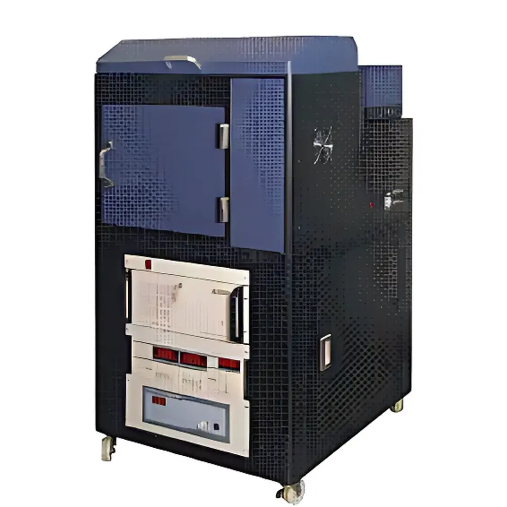
ZOLIX PMEye-3000 Photoluminescence Spectral Imaging Mapping System
| Brand | ZOLIX |
|---|---|
| Origin | Beijing, China |
| Manufacturer Type | Manufacturer |
| Product Origin | Domestic (China) |
| Model | PMEye-3000 |
| Pricing | Upon Request |
Overview
The ZOLIX PMEye-3000 Photoluminescence Spectral Imaging Mapping System is a high-precision, modular platform engineered for quantitative spatial-spectral characterization of semiconductor materials. It operates on the physical principle of photoluminescence (PL): when a semiconductor sample is excited by monochromatic laser radiation, electrons are promoted to higher energy states; upon radiative recombination, photons are emitted whose wavelength distribution reflects fundamental material properties—including bandgap energy, crystalline quality, defect density, carrier lifetime, and compositional uniformity. Unlike conventional single-point PL spectrometers, the PMEye-3000 integrates synchronized 2D motorized stage scanning with high-resolution spectroscopic detection to generate pixel-resolved spectral datasets across wafer-scale samples (up to 200 × 200 mm, accommodating 8-inch substrates). Each acquired spectrum is georeferenced, enabling full spectral cube (λ–x–y) reconstruction and subsequent 3D visualization of intensity, peak wavelength, FWHM, or integrated emission bands—critical for process development, failure analysis, and statistical process control in compound semiconductor manufacturing.
Key Features
- Automated PL spectral mapping with up to 180 measurement points per second
- Spatial resolution down to 50 µm via precision XYZ stage and optimized optical path design
- Spectral resolution of 0.1 nm (at 1200 grooves/mm grating), supporting fine-structure analysis of excitonic peaks and defect-related emissions
- Dual-mode acquisition: DC mode for routine intensity mapping; AC lock-in mode for enhanced signal-to-noise ratio in low-yield or trap-dominated materials
- Real-time excitation laser power monitoring and dynamic intensity normalization to eliminate source drift-induced artifacts
- Modular excitation architecture: supports up to two internal lasers (standard: 405 nm) plus one external port; optional wavelengths include 325 nm, 442 nm, 532 nm, 785 nm, and 808 nm
- Vacuum-assisted sample mounting for non-damaging, repeatable positioning of fragile epitaxial wafers and thin films
- Integrated cryogenic accessory option for temperature-dependent PL studies from 25 K to 300 K
- Ergonomic upright configuration with retractable peripheral platform, castor-mounted base, and human-centered workstation geometry
Sample Compatibility & Compliance
The PMEye-3000 accommodates rigid and semi-rigid planar substrates including GaN, InGaN, AlGaAs, SiC, perovskite thin films, quantum dot arrays, and CIGS solar absorbers. Its vacuum chuck ensures flatness and positional repeatability (< ±1 µm) across 8-inch wafers without mechanical clamping stress. The system complies with general laboratory safety standards (IEC 61010-1) and supports traceable calibration protocols aligned with ISO/IEC 17025 requirements for analytical instrument validation. While not certified for GMP production environments out-of-the-box, its software architecture enables audit trail configuration, user access control, and electronic signature readiness—facilitating alignment with FDA 21 CFR Part 11 and GLP documentation workflows when deployed in regulated R&D labs.
Software & Data Management
The proprietary MEye-3000 software provides a unified interface for instrument control, real-time data acquisition, and multidimensional analysis. Core capabilities include: single-point spectral acquisition; wavelength-specific X–Y intensity mapping; full-spectrum mapping over user-defined λ ranges; automated peak fitting (centroid, FWHM, asymmetry); integration-based quantification; and 3D surface rendering with customizable colormaps and contour overlays. All raw spectra are stored in HDF5 format with embedded metadata (excitation wavelength, power, integration time, stage coordinates, temperature). Batch processing scripts support spectral deconvolution, background subtraction, and statistical outlier detection across large wafer maps. Export options include CSV, ASCII, and image formats (PNG, TIFF) compatible with MATLAB, Python (NumPy/Pandas), and commercial data analytics platforms.
Applications
- LED epitaxial wafer screening: identification of lateral nonuniformity in quantum well composition, thickness, and strain
- Solar cell material assessment: mapping of carrier diffusion length, defect clustering, and interfacial recombination at grain boundaries
- Perovskite film homogeneity evaluation: correlation of PL quantum yield gradients with spin-coating parameters
- 2D material characterization: spatial variation of exciton binding energy and valley polarization in MoS₂ or WSe₂ monolayers
- QC/QA in semiconductor foundries: pass/fail criteria based on spectral centroid deviation, FWHM thresholding, or integrated intensity variance
- Fundamental low-temperature physics: tracking of bandgap renormalization, phonon coupling, and localized state activation as a function of cryogenic temperature
FAQ
What laser wavelengths are supported natively?
The standard configuration includes one internally mounted 405 nm diode laser. Optional internal lasers include 442 nm, 532 nm, 785 nm, and 808 nm. An external port supports integration of a 325 nm HeCd laser.
Can the system perform time-resolved PL measurements?
No—the PMEye-3000 is designed for steady-state spectral mapping. Time-resolved capability requires pulsed excitation sources and gated detection hardware, which are not part of this platform.
Is vacuum compatibility available for in-situ measurements?
The sample chamber is ambient-air compatible. A dedicated vacuum-compatible stage and sealed optical viewport can be custom-integrated upon request, but are not included in the base configuration.
How is spectral calibration maintained over long-term operation?
The system includes an onboard neon lamp for periodic wavelength calibration and a reference photodiode for intensity linearity verification. Calibration routines are accessible through the software and recommended before each mapping session.
Does the software support batch analysis of multiple wafers?
Yes—MEye-3000 includes project-level organization tools, automated report generation (PDF/HTML), and scripting interfaces for cross-wafer statistical comparison using user-defined metrics.


")