ZOLIX SPM300 Semiconductor Wafer Stress & Carrier Concentration Mapping System
| Brand | ZOLIX |
|---|---|
| Origin | Beijing, China |
| Manufacturer Type | Original Equipment Manufacturer (OEM) |
| Product Category | Optical Defect Inspection System for Semiconductor Wafers |
| Model | SPM300 |
| Excitation Wavelength | 532 nm (standard), 275 nm UV optional |
| Laser Power | 50 mW |
| Autofocus Precision | < 0.2 µm |
| Spatial Resolution | < 2 µm |
| Raman Shift Range | 80–9000 cm⁻¹ |
| Spectral Resolution | < 2.0 cm⁻¹ |
| Mapping Scan Area | > 300 × 300 mm² |
| Minimum Step Size | 1 µm |
| Compatible Wafer Sizes | 2", 4", 6", 8" (12" customizable) |
| Objective | 100× semi-apochromatic |
| Detection Mode | Confocal Raman + PL + Fluorescence Lifetime (TCSPC) |
| Software Compliance | Supports ASTM E2912, ISO/IEC 17025 workflows, GLP/GMP audit trail logging per FDA 21 CFR Part 11 requirements |
Overview
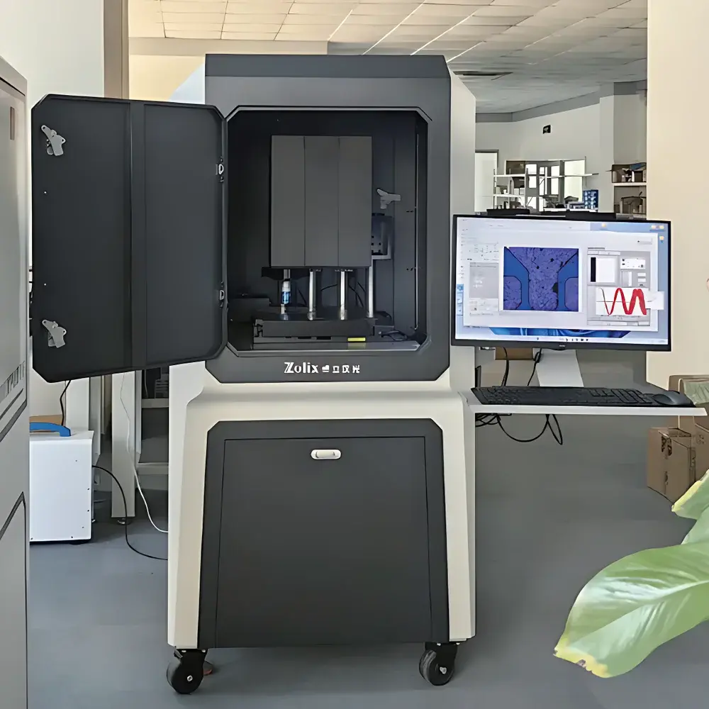
The ZOLIX SPM300 is a fully integrated, confocal micro-Raman and photoluminescence (PL) mapping platform engineered for non-destructive, quantitative characterization of mechanical stress and carrier concentration in semiconductor wafers. It operates on the physical principle of inelastic light scattering—Raman spectroscopy—to detect lattice strain-induced shifts in vibrational modes (e.g., the 520 cm⁻¹ Si phonon mode), while simultaneously acquiring time-resolved fluorescence lifetime (TCSPC) and spectral intensity data to extract carrier density via band-edge emission analysis. Unlike contact-based or X-ray diffraction methods, the SPM300 enables high-spatial-resolution (<2 µm), real-time, in-line compatible assessment without sample preparation or vacuum requirements. Its dual-wavelength excitation architecture (532 nm standard + 275 nm UV optional) supports both bulk silicon stress mapping and deep-UV-sensitive wide-bandgap materials—including SiC, GaN, and AlGaN—where conventional visible excitation suffers from poor signal-to-noise or strong background luminescence.
Key Features
- Automated confocal laser focusing with proprietary UV-assisted defocus sensing: maintains sub-0.2 µm axial stability across full wafer scans, enabling reliable surface tracking on warped or patterned substrates.
- Multi-modal optical detection: simultaneous acquisition of brightfield microscopy, darkfield UV fluorescence imaging, and infrared darkfield PL imaging—optimized for dislocation, stacking fault, and defect cluster localization.
- Modular spectrometer architecture: 320 mm focal-length Czerny–Turner monochromator coupled to a back-illuminated CCD array, delivering <2.0 cm⁻¹ spectral resolution across 80–9000 cm⁻¹ range.
- Motorized XYZ stage with 300 × 300 mm² travel range and 1 µm step resolution; vacuum chuck-compatible 8-inch (12-inch optional) electrostatic wafer holder.
- Fully software-controlled operation: unified GUI for coordinate-based region-of-interest (ROI) definition, point-by-point spectral acquisition, and automated Raman/PL lifetime mapping.
- Onboard TCSPC algorithm suite: IRF-free rising-edge deconvolution, multi-exponential decay fitting (up to 4 components), photon-counting uncertainty correction, and residual-weighted χ² evaluation for robust lifetime quantification.
Sample Compatibility & Compliance
The SPM300 is validated for use with bare and patterned wafers of Si, Ge, SiC, GaN, InP, and compound III–V heterostructures. Its optical design meets ISO 14644-1 Class 5 cleanroom compatibility standards when installed with appropriate enclosures. The system adheres to semiconductor metrology traceability frameworks aligned with ASTM E2912 (Standard Practice for Raman Spectroscopy of Silicon Wafers) and supports calibration protocols referenced in GB/T 43493.3–2023—the Chinese national standard for non-destructive photoluminescence defect identification in SiC epitaxial wafers. All software modules implement audit-trail logging, electronic signature support, and user-role-based access control to satisfy FDA 21 CFR Part 11 and ISO/IEC 17025 documentation requirements for GLP/GMP environments.
Software & Data Management
The VisualSpectra™ software suite provides end-to-end spectral data handling—from raw acquisition to quantitative parametric mapping. Core capabilities include background subtraction, spectral smoothing, stitching correction, and unit conversion (cm⁻¹ ↔ nm ↔ eV). Peak fitting employs constrained Gaussian–Lorentzian hybrid models to extract position, FWHM, and integrated intensity for each Raman or PL band. Dedicated modules perform: (i) stress quantification using material-specific calibration coefficients (Si: −0.32 cm⁻¹/MPa; GaN: −2.1 cm⁻¹/GPa); (ii) carrier concentration estimation via Burstein–Moss shift analysis of near-band-edge PL; (iii) crystallinity index calculation from Raman peak asymmetry and FWHM trends; and (iv) TCSPC lifetime distribution mapping. Advanced multivariate analysis includes PCA decomposition and k-means clustering, enabling unsupervised classification of spatially heterogeneous regions based on spectral signatures. All processing pipelines are scriptable (Python API), exportable as SOP-compliant RECIPE files, and integrable with factory MES systems via OPC UA.
Applications
The SPM300 serves critical process control functions across front-end semiconductor fabrication: monitoring residual stress gradients after rapid thermal annealing (RTA), evaluating epitaxial layer uniformity in SiC power device wafers, quantifying strain relaxation in strained-Si CMOS channels, detecting threading dislocations in GaN-on-sapphire LEDs, and correlating carrier lifetime with defect density in photovoltaic-grade silicon. It further supports R&D applications such as strain-engineered 2D material heterostructures, quantum dot ensemble characterization, and dopant activation profiling in ion-implanted layers. Its ability to co-register structural (Raman), electronic (PL intensity/shift), and dynamic (lifetime) information at micron-scale resolution makes it uniquely suited for root-cause analysis of yield-limiting defects in advanced node manufacturing.
FAQ
What materials can the SPM300 characterize for stress and carrier concentration?
The system is optimized for single-crystal and polycrystalline semiconductors including Si, Ge, SiC, GaN, AlN, InP, and related alloys. Custom calibration packages are available for emerging materials such as β-Ga₂O₃ and hexagonal boron nitride.
Does the SPM300 support automated defect classification?
Yes—VisualSpectra™ includes supervised and unsupervised machine learning modules that classify defect types (e.g., dislocations vs. stacking faults) based on spectral shape, lifetime decay kinetics, and spatial correlation patterns.
Can the system be integrated into a fab’s automation infrastructure?
It supports SECS/GEM protocol compliance and offers OPC UA server functionality for bidirectional communication with host MES/SCADA systems, enabling recipe-driven automated metrology runs.
Is the software compliant with regulatory data integrity requirements?
All software modules implement ALCOA+ principles: attributable, legible, contemporaneous, original, accurate, complete, consistent, enduring, and available—with full electronic audit trails, role-based permissions, and 21 CFR Part 11-compliant digital signatures.
What level of technical support and calibration services are provided?
ZOLIX offers on-site installation qualification (IQ), operational qualification (OQ), and performance qualification (PQ) services; annual NIST-traceable wavelength and intensity calibration; and remote diagnostics with SLA-backed response times.


