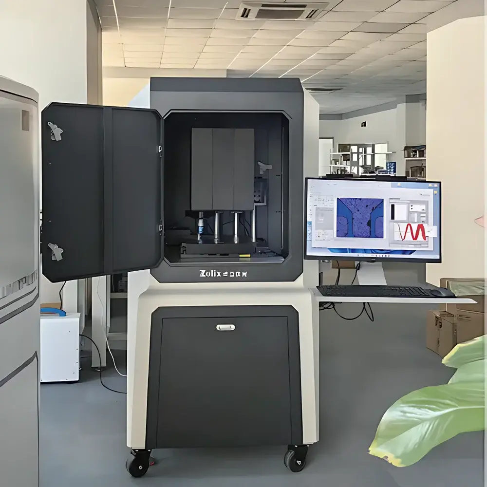
ZOLIX SPM900 Wafer-Scale Photoluminescence & Minority Carrier Lifetime Mapping System
| Brand | ZOLIX |
|---|---|
| Origin | Beijing, China |
| Manufacturer Type | Original Equipment Manufacturer (OEM) |
| Product Category | Optical Defect Inspection System for Semiconductor Wafers |
| Model | SPM900 |
| Instrument Type | Steady-State and Time-Resolved Photoluminescence (PL) Mapping System |
| Excitation Wavelengths | 213 nm, 266 nm, 375 nm, 405 nm |
| Autofocus Accuracy | < 0.2 µm |
| Scan Range | > 300 × 300 mm² |
| Minimum Spatial Resolution | 1 µm |
| Compatible Wafer Sizes | 2", 4", 6", 8" (12" optional) |
| Objective Lenses | UV (5×), NUV (20×/100×), Visible (20×/50×/100×) |
| Spectrometer | 320 mm focal length, 1200 g/mm grating, spectral resolution ≤ 0.2 nm |
| PL Lifetime Range | 50 ps – 1 ms |
| Lifetime Precision | 8 ps |
| Detection Modes | Confocal steady-state PL, time-resolved PL (TRPL), fluorescence lifetime imaging (FLIM), Raman mapping, photocurrent mapping |
Overview
The ZOLIX SPM900 Wafer-Scale Photoluminescence & Minority Carrier Lifetime Mapping System is an integrated optical metrology platform engineered for non-destructive, high-resolution characterization of semiconductor wafers during process development and quality control. It combines confocal photoluminescence (PL) spectroscopy with time-resolved detection to simultaneously map spatial variations in luminescence intensity, peak wavelength, full width at half maximum (FWHM), carrier recombination dynamics, and minority carrier lifetime across full 2–8 inch wafers. The system operates on the physical principle of photoluminescence—where incident photons excite electrons from the valence band to the conduction band, followed by radiative recombination emitting photons whose energy distribution reflects material band structure, defect states, impurity levels, and lattice strain. Unlike contact-based electrical methods, PL mapping provides intrinsic, label-free insight into optoelectronic quality without perturbing device integrity—making it essential for GaN, SiC, InGaN, perovskite, and AlGaN epitaxial layers used in LEDs, laser diodes, power electronics, and photovoltaics.
Key Features
- Automated confocal scanning architecture with real-time surface tracking via proprietary laser-assisted defocus sensing—enabling sub-200 nm axial focus stability over full-wafer topography including warpage and step height variations.
- Multi-wavelength excitation capability (213 nm, 266 nm, 375 nm, 405 nm) with dedicated UV, near-UV, and visible objectives optimized for diffraction-limited spot size and collection efficiency across wide-bandgap materials.
- Dual-path fluorescence collection: coaxial (forward) and lateral (side) detection channels—critical for materials governed by dipole emission selection rules (e.g., AlGaN), where out-of-plane emission is suppressed.
- Modular spectrometer subsystem featuring a 320 mm Czerny–Turner monochromator with 1200 g/mm grating and back-illuminated CCD or EMCCD array detector—delivering spectral resolution ≤ 0.2 nm at 500 nm.
- Time-correlated single-photon counting (TCSPC) module with 8 ps instrument response function (IRF) deconvolution algorithm—supporting multi-exponential lifetime fitting (up to 4 components) without empirical IRF measurement.
- Fully software-defined operation: unified GUI for wafer alignment, region-of-interest definition, point-scan, line-scan, area-mapping, and synchronized data acquisition across PL, TRPL, Raman, and photocurrent modalities.
Sample Compatibility & Compliance
The SPM900 accommodates standard semiconductor substrates—including Si, sapphire, SiC, and quartz—with vacuum-compatible chuck options (8-inch electrostatic chuck; 12-inch customizable). Its optical design complies with ISO 14644-1 Class 5 cleanroom integration requirements and supports GMP/GLP-aligned workflows through audit-trail-enabled software logging (user actions, parameter changes, calibration timestamps). While not certified to IEC 61000-4 electromagnetic compatibility standards out-of-the-box, the system meets CE marking criteria for laboratory instrumentation when installed per manufacturer grounding and shielding guidelines. Data output formats (HDF5, CSV, TIFF) are compatible with ASTM E2913-21 digital reporting conventions for semiconductor metrology traceability.
Software & Data Management
The VISUALSPECTRA software suite provides end-to-end spectral image processing: background subtraction, spectral smoothing, stitching correction, unit conversion (nm → eV), peak fitting (Gaussian, Lorentzian, Voigt), and multivariate analysis (PCA, k-means clustering). Advanced modules include stress quantification from Raman shifts (calibrated for Si, GaN, SiC using NIST-traceable reference samples), carrier concentration estimation via PL quenching modeling, crystallinity assessment from FWHM trends, and TCSPC-derived lifetime component decomposition. All processing pipelines support batch execution across entire wafer maps and export to industry-standard formats for integration with MES (Manufacturing Execution Systems) or statistical process control (SPC) platforms. Optional FDA 21 CFR Part 11 compliance packages include electronic signatures, role-based access control, and immutable audit logs.
Applications
- Quantitative compositional mapping of ternary/quaternary alloys (e.g., InxGa1−xN) via PL peak energy calibration against known bandgap–composition relationships.
- Spatially resolved identification and semi-quantitative profiling of transition-metal impurities (Fe, Cr, Cu) and residual dopants (Mg, Si) through characteristic zero-phonon lines and phonon sidebands.
- Defect density estimation using non-radiative recombination ratio (INR/IR) derived from integrated PL intensity and lifetime decay kinetics—correlating with threading dislocation density in GaN epilayers.
- Process validation for MOCVD/MBE growth uniformity, annealing efficacy, etch-induced damage assessment, and passivation layer integrity evaluation.
- Correlative metrology: overlaying PL lifetime maps with SEM, AFM, or XRD data to isolate microstructural origins of optoelectronic degradation.
FAQ
What wafer sizes does the SPM900 support?
Standard configuration supports 2-inch to 8-inch wafers; 12-inch compatibility is available as a factory-customized option with extended scan range and reinforced stage mechanics.
Can the system perform both steady-state and time-resolved PL on the same platform?
Yes—the hardware architecture integrates dual detection paths and synchronized TCSPC electronics, enabling seamless switching between continuous-wave and pulsed excitation modes without realignment.
Is spectral calibration traceable to NIST standards?
All spectrometer calibrations are performed using NIST-traceable Hg/Ar/Ne emission lamps, with certificate-of-calibration documentation provided upon installation and annually during preventive maintenance.
How is autofocus maintained across warped or patterned wafers?
The proprietary laser defocus sensor operates in parallel with PL acquisition, updating focus position at ≥100 Hz during raster scanning—compensating for up to ±100 µm vertical deviation without loss of spectral fidelity.
Does the software support custom spectral analysis algorithms?
Yes—VISUALSPECTRA includes Python API hooks and a plugin framework for integrating user-defined fitting routines, machine learning models, or proprietary material-specific interpretation logic.


