ZOLIX UHV-Integrated Confocal Raman Microspectroscopy System
| Brand | ZOLIX |
|---|---|
| Origin | Beijing, China |
| Manufacturer Type | OEM Manufacturer |
| Origin Category | Domestic (China) |
| Model | Confocal Raman Microscope Module |
| Instrument Type | Confocal Raman Spectrometer |
| Vacuum Compatibility | Ultra-High Vacuum (UHV, ≤1×10⁻¹⁰ mbar) |
| Optical Integration | External Modular Microscope Assembly with UHV Viewport Coupling |
| Working Distance | Up to 120 mm |
| Laser Wavelength Options | 532 nm, 633 nm, 785 nm (configurable) |
| Spectral Resolution | <1 cm⁻¹ (with high-throughput Czerny–Turner monochromator) |
| Detector | Back-illuminated CCD or EMCCD (optional) |
| Objective Lenses | Long-working-distance, UHV-compatible, aberration-corrected objectives (e.g., 20×, 50×, 100×, NA up to 0.9) |
| Autofocus | Integrated laser displacement sensor + piezo-driven objective stage |
| Confocality | Pinhole-based spatial filtering with motorized alignment |
| Window Compensation | Real-time optical path correction for viewport glass thickness-induced wavefront distortion |
| Data Compliance | Supports timestamped spectral metadata, audit-ready acquisition logs |
Overview
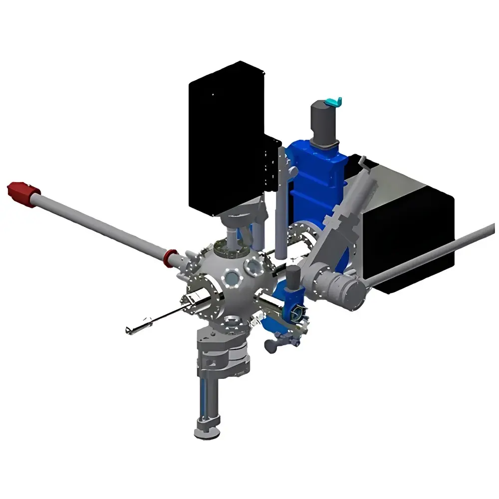
The ZOLIX UHV-Integrated Confocal Raman Microspectroscopy System is an engineered solution for in-situ, non-destructive characterization of atomically thin materials, epitaxial thin films, and vacuum-deposited heterostructures within ultra-high vacuum (UHV) environments. Unlike conventional Raman systems requiring sample transfer and atmospheric exposure, this system implements a fully externalized optical architecture: the entire confocal microscope module—including excitation optics, high-numerical-aperture long-working-distance objectives, pinhole-based spatial filtering, laser displacement autofocus, and spectrometer coupling—is physically isolated from the UHV chamber. Optical access is achieved exclusively through a precision-machined viewport, enabling diffraction-limited focusing onto samples maintained at base pressures ≤1×10⁻¹⁰ mbar. The system operates on standard confocal Raman principles: monochromatic laser light is focused onto the sample surface; inelastically scattered photons are collected through the same objective, spectrally dispersed via a high-throughput Czerny–Turner monochromator, and detected using thermoelectrically cooled back-illuminated CCD or EMCCD sensors. This design eliminates hydrocarbon contamination, preserves surface integrity during growth-interrupt analysis, and supports real-time feedback in molecular beam epitaxy (MBE), atomic layer deposition (ALD), and van der Waals heterostructure assembly workflows.
Key Features
- Modular external optical head: Fully decoupled from UHV chamber—no internal optical components, zero outgassing risk, no vacuum compatibility constraints on detectors or gratings.
- Long-working-distance optics: Standard 120 mm working distance accommodates thick shielding flanges, cryogenic stages, and multi-probe UHV manipulators without optical interference.
- Aberration-compensated viewport interface: Real-time optical path correction algorithm compensates for spherical and chromatic distortions induced by viewport glass thickness (up to 25 mm), ensuring diffraction-limited spot size (<0.5 µm FWHM at 532 nm).
- Automated confocal alignment: Motorized pinhole positioning synchronized with objective Z-stage and laser focus tracking ensures consistent depth sectioning across variable sample topographies.
- Configurable excitation & detection: Interchangeable lasers (532/633/785 nm), selectable grating densities (1200–2400 grooves/mm), and detector options (standard CCD, deep-depletion CCD, or EMCCD) support trade-offs between signal-to-noise ratio, spectral resolution, and fluorescence suppression.
- UHV serviceability: Entire optical module mounts via kinematic interface—removable as a single unit for chamber bakeout (≥150 °C); repeatable sub-5 µm repositioning accuracy after reinstallation.
Sample Compatibility & Compliance
The system is validated for use with conductive and insulating substrates including Si(100), sapphire, h-BN, graphene/SiO₂, and transition metal dichalcogenide monolayers. It complies with ISO 17025 calibration traceability requirements when paired with NIST-traceable Raman shift standards (e.g., silicon 520.7 cm⁻¹ peak). All optical components meet UHV material specifications per ASTM E1557 (outgassing rate <1×10⁻¹² Pa·m³/s·cm²). Mechanical interfaces conform to CF-100 and KF-40 flange standards. The system architecture supports integration into larger UHV interconnect platforms compliant with EUROPEN (European Platform for UHV Nanoscience) interoperability guidelines.
Software & Data Management
Control and acquisition are managed via ZOLIX SpectraSuite™ v5.x, a Windows-based platform supporting multi-instrument synchronization (e.g., lock-in amplifiers, temperature controllers, piezo scanners). Raw spectra are stored in HDF5 format with embedded metadata: laser power (measured in situ via integrated photodiode), exposure time, grating position, objective ID, viewport temperature, and vacuum pressure timestamp. Audit trails record all parameter changes with user ID and UTC timestamps. Optional FDA 21 CFR Part 11 compliance package provides electronic signatures, role-based access control, and immutable acquisition logs suitable for GLP/GMP-regulated thin-film QC laboratories.
Applications
- In-situ monitoring of 2D material transfer quality: Quantitative mapping of strain distribution, layer count, and defect density in graphene and MoS₂ prior to device fabrication.
- Epitaxial interface analysis: Detection of interfacial phonon modes and interdiffusion signatures in GaAs/AlGaAs quantum wells during MBE growth pauses.
- Catalyst surface evolution: Tracking adsorbate-induced Raman shifts on Pt(111) under controlled UHV gas dosing and thermal cycling.
- Topological insulator characterization: Resolving Dirac cone-related Raman features in Bi₂Se₃ while maintaining native surface termination.
- Correlative UHV metrology: Synchronized acquisition with low-energy electron diffraction (LEED) or scanning tunneling microscopy (STM) signals for multimodal structure–property correlation.
FAQ
Can the system be retrofitted to existing UHV chambers?
Yes—the optical module interfaces via standard CF-100 or DN160 flanges; custom viewport adapters are available for non-standard geometries.
Is vacuum-compatible anti-reflection coating applied to all optical elements?
All external-facing optics (objectives, tube lenses, dichroics) feature ion-beam-sputtered AR coatings optimized for 400–1000 nm, with residual reflectivity <0.25% per surface.
What is the minimum resolvable Raman shift difference under standard configuration?
With 1800 g/mm grating and 1024×128-pixel CCD, full-width half-maximum resolution is ≤0.8 cm⁻¹ at 532 nm excitation (verified using neon emission lines).
Does the autofocus system function reliably on highly reflective or transparent substrates?
Yes—the integrated laser displacement sensor operates independently of Raman signal intensity and maintains ±50 nm repeatability across Si, sapphire, and CaF₂ substrates.
Are spectral calibration certificates provided with each system?
Each instrument ships with a factory calibration report referencing NIST SRM 2241 (silicon) and SRM 2242 (polystyrene), traceable to BIPM standards via NIM (National Institute of Metrology, China).