HORIBA HCLUE High-Efficiency Cathodoluminescence Spectrometer
| Brand | HORIBA |
|---|---|
| Origin | France |
| Manufacturer Type | Manufacturer |
| Import Status | Imported |
| Model | HCLUE |
| Pricing | Upon Request |
Overview
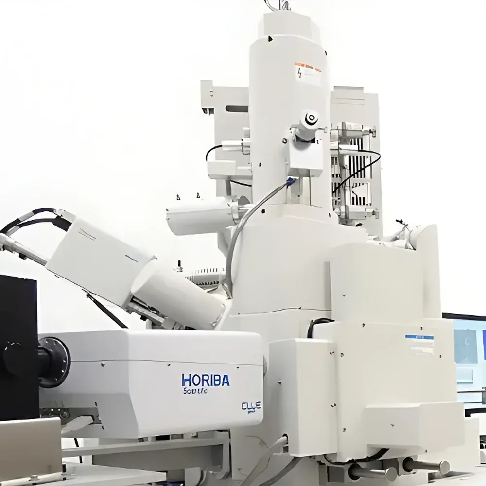
The HORIBA HCLUE is a high-efficiency cathodoluminescence (CL) spectrometer engineered for integration with scanning electron microscopes (SEM) and transmission electron microscopes (TEM). It operates on the fundamental principle of cathodoluminescence—wherein incident electron beam energy excites luminescent emission from solid-state materials, and the resulting photons are collected, dispersed, and spectrally resolved via optimized mirror-coupled optics and high-throughput spectrograph modules. Unlike conventional CL systems relying on fiber coupling or inefficient light collection geometries, the HCLUE employs direct reflective coupling between the microscope chamber and the spectrometer entrance, minimizing photon loss and preserving spatial fidelity. This architecture enables nanoscale spectral mapping with sub-100 nm spatial resolution when synchronized with SEM beam scanning, making it particularly suited for correlative structural–optical analysis of semiconductors, wide-bandgap oxides, geological minerals, and biomaterials.
Key Features
- Direct mirror-based optical coupling to SEM/TEM chambers for maximum photon throughput and minimal aberration
- High-sensitivity spectrograph module built upon Jobin Yvon optical design heritage, featuring precision-aligned diffraction gratings and thermally stabilized optical benches
- Flexible configuration options: selectable focal lengths (320 mm, 500 mm, or 550 mm) to balance spectral resolution (down to 0.05 nm FWHM at 500 mm) and throughput
- Dual-detector capability supporting simultaneous UV–NIR coverage from 185 nm to 2500 nm—enabling full-band characterization without mechanical reconfiguration
- Multi-modal acquisition modes: point-spectrum acquisition, line scans, and hyperspectral CL imaging with pixel-resolved spectral stacks
- SWIFT™ ultrafast imaging mode for real-time CL mapping at frame rates up to 100 fps, compatible with standard SEM scan generators
Sample Compatibility & Compliance
The HCLUE accommodates a broad range of solid-state specimens—including bulk crystals, thin films, nanostructures, polished mineral sections, and biological tissue preparations—without requiring conductive coating in many cases due to its high signal-to-noise performance. Its vacuum-compatible design ensures seamless operation under standard SEM operating pressures (10⁻⁴ to 10⁻⁶ Pa). The system complies with ISO/IEC 17025 requirements for analytical instrument validation and supports GLP/GMP-compliant workflows through traceable calibration protocols (NIST-traceable wavelength and intensity standards available). All firmware and control logic adhere to IEC 61508 functional safety guidelines for laboratory instrumentation.
Software & Data Management
Control and data acquisition are managed via HORIBA’s LabSpec 6 platform, which provides integrated SEM synchronization, real-time spectral preview, and batch processing of hyperspectral datasets. The software supports ASTM E131-compliant spectral metadata embedding (including excitation conditions, detector gain, grating position, and calibration timestamps) and exports fully annotated spectra in JCAMP-DX, ASCII, and HDF5 formats. Audit trails, user access controls, and electronic signatures comply with FDA 21 CFR Part 11 requirements for regulated environments. Raw spectral cubes (x, y, λ) can be imported into Python (via h5py), MATLAB, or commercial tools such as ENVI for multivariate analysis, PCA decomposition, or band-edge fitting.
Applications
- Semiconductor & optoelectronics: Defect identification in GaN, SiC, and perovskite thin films; quantum well localization analysis; dopant distribution mapping
- Geosciences & mineralogy: Zircon geochronology via U–Th–Pb luminescence zoning; dolomite/calcite differentiation in carbonate sequences; diamond nitrogen-aggregate typing
- Materials science: Phase segregation in multiferroics; grain-boundary recombination activity in polycrystalline oxides; plasmonic hot-spot mapping in metal–dielectric nanostructures
- Life sciences: Calcium phosphate biomineralization studies; rare-earth-doped bioimaging probes; fossilized tissue luminescence fingerprinting
- Forensics: Trace evidence discrimination (e.g., glass refractive index profiling, pigment identification in paint chips)
FAQ
What vacuum interface options are available for SEM integration?
Standard configurations include CF-63 and CF-100 flanges compatible with JEOL, Thermo Fisher, Zeiss, and Hitachi SEM platforms. Custom feedthroughs for differential pumping stages are available upon request.
Can the HCLUE be used with TEM instruments?
Yes—dedicated TEM-compatible versions with modified mirror geometry and low-voltage electron optics shielding are offered for 200–300 kV transmission systems.
Is spectral calibration traceable to national standards?
Wavelength calibration uses NIST-traceable Hg–Ar and Ne emission lines; radiometric calibration employs certified tungsten halogen sources with ±2% uncertainty across 200–1100 nm.
How is spatial registration maintained during CL mapping?
Beam position coordinates are acquired synchronously with spectral data via SEM digital scan generator outputs, enabling sub-pixel registration accuracy when combined with stage encoder feedback.
Does the system support time-resolved CL measurements?
Time-correlated single-photon counting (TCSPC) is supported via optional PicoQuant or Becker & Hickl modules interfaced through TTL-gated detection channels.
Related Products