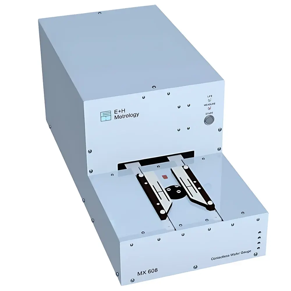
Endress+Hauser MX608 Wafer Thickness & Resistivity Metrology System
| Brand | Endress+Hauser Metrology |
|---|---|
| Origin | Germany |
| Model | MX608 |
| Wafer Diameter Support | 150 mm, 200 mm, 300 mm |
| Thickness Range | 500–800 µm |
| Max Warp | 100 µm |
| Resistivity Range | 0.001–200 Ω·cm |
| Thickness Accuracy | ±0.3 µm |
| TTV Accuracy | ±0.1 µm |
| Thickness Repeatability | ±0.05 µm |
| Resistivity Accuracy | ±1% (0.001–80 Ω·cm), ±5% (200 Ω·cm) |
| Resistivity Repeatability | ±0.2% (0.001–80 Ω·cm), ±2% (200 Ω·cm) |
| Edge Measurement Capability | up to 130 mm (150 mm wafers), up to 180 mm (200 mm wafers) |
| Single-Point Measurement Time | ~7 s |
| Full-Surface Scan (130/180 points) | ~10 s |
| Multi-Angle Radial Scan (18 scans @ 10° intervals) | ~3 min |
| Carrier Type Detection | P/N identification via Surface Photovoltage (SPV) |
Overview
The Endress+Hauser MX608 Wafer Thickness & Resistivity Metrology System is a fully automated, non-contact inline metrology platform engineered for high-precision characterization of silicon wafers during front-end semiconductor fabrication. It integrates three complementary physical measurement principles—eddy current sensing, differential capacitive displacement, and surface photovoltage (SPV)—to simultaneously quantify bulk electrical and geometric properties critical to process control and yield management. Unlike contact-based or destructive methods, the MX608 operates without mechanical loading or surface contamination risk, ensuring compatibility with bare, polished, epitaxial, or oxide-coated wafers across 150 mm, 200 mm, and 300 mm diameters. Its architecture supports integration into cleanroom automation environments (SECS/GEM compliant), enabling real-time feedback for furnace calibration, epitaxy uniformity verification, and post-diffusion resistivity profiling.
Key Features
- Triple-sensor fusion architecture: Eddy current coil for resistivity and carrier type (P/N), dual capacitive probes for thickness, bow, warp, and total thickness variation (TTV), and SPV module for non-contact carrier polarity determination.
- Sub-micron geometric resolution: Thickness accuracy ±0.3 µm, TTV accuracy ±0.1 µm, and repeatability better than ±0.05 µm—validated per ISO 21243 and SEMI MF1530 standards.
- Wide resistivity dynamic range: Quantifies resistivity from ultra-low doped (0.001 Ω·cm) to heavily compensated material (200 Ω·cm), with traceable calibration against NIST-traceable silicon reference wafers.
- Full-wafer spatial mapping: Supports single-point, radial line scan (up to 180 points), and multi-angle azimuthal scans (e.g., 18×10° rotations) to generate contour maps of thickness, resistivity, and flatness per SEMI MF1390.
- Automated edge exclusion and notch/flat detection: Configurable measurement zones aligned to wafer fiducials; no manual alignment required.
- Robust environmental compensation: Integrated temperature and humidity sensors enable real-time correction for thermal drift in cleanroom conditions (Class 100–1000).
Sample Compatibility & Compliance
The MX608 is validated for use with prime, test, and monitor wafers—including CZ, FZ, and epitaxial silicon—with or without native oxide, thermal oxide (<10 nm), or anti-reflective coatings. It complies with key industry standards including SEMI MF1530 (resistivity measurement), SEMI MF1390 (wafer geometry), ISO 21243 (capacitive thickness metrology), and ASTM F1530 (eddy current conductivity testing). All measurement algorithms are deterministic and auditable, supporting GLP/GMP workflows with full electronic record retention. The system meets IEC 61000-6-2 (immunity) and IEC 61000-6-4 (emission) requirements for semiconductor fab floor deployment.
Software & Data Management
Controlled via Endress+Hauser’s proprietary MetroSuite MX software, the MX608 provides a secure, role-based interface compliant with FDA 21 CFR Part 11 and EU Annex 11. Audit trails log all user actions, parameter changes, calibration events, and raw data exports. Measurement reports export natively to CSV, XML, and SPC-compliant formats (e.g., JMP, Minitab), with optional integration into factory MES via SECS/GEM or OPC UA. Calibration certificates include uncertainty budgets per GUM (JCGM 100), and software validation packages (IQ/OQ/PQ documentation) are available for regulated environments.
Applications
- Pre-epitaxy substrate qualification: Verifying baseline resistivity uniformity and thickness before epi-deposition.
- In-line furnace monitoring: Tracking dopant diffusion profiles and sheet resistance evolution across thermal cycles.
- Post-CMP thickness verification: Assessing removal uniformity and detecting subsurface damage via TTV/bow correlation.
- Carrier type screening: Rapid P/N classification of reclaimed or recycled wafers prior to reuse.
- Process window qualification: Statistical analysis of resistivity and thickness Cpk values across lot-to-lot production.
- Reference wafer certification: Supporting internal lab traceability for resistivity and geometry standards.
FAQ
Does the MX608 require physical contact with the wafer surface?
No. All measurements are performed non-invasively using electromagnetic (eddy current), electrostatic (capacitive), and optoelectronic (SPV) principles.
Can the system measure wafers with thin dielectric layers (e.g., SiO₂ < 5 nm)?
Yes. The eddy current and capacitive modules are calibrated to compensate for native and thermally grown oxides up to 10 nm thick.
Is calibration traceable to national metrology institutes?
Yes. Factory calibrations use NIST-traceable silicon reference wafers; on-site recalibration kits include certified geometry and resistivity standards.
What level of cleanroom compatibility does the MX608 support?
The system is rated for Class 100 (ISO 5) environments and includes HEPA-filtered purge air options for optical path protection.
How is data integrity ensured during long-term deployment?
MetroSuite MX implements write-once audit logs, digital signatures for exported reports, and configurable retention policies aligned with ISO 17025 data lifecycle requirements.


