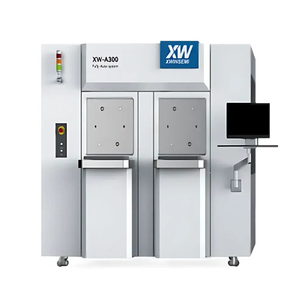
Aiyao XW-A300 Wafer Geometry Metrology System for Thickness (TTV), Bow/Warp, and Surface Roughness
| Brand | Aiyao Instruments |
|---|---|
| Origin | Taiwan |
| Model | XW-A300 |
| Measurement Principles | Spectral Interferometry (IR), White-Light Interferometry (WLI), Optical Reflectometry |
| Sample Compatibility | 4″–12″ wafers |
| Probe Configuration | Single or Dual (top/bottom) |
| Compliance | SEMI S2/S8 |
| Motion Platform | Air-bearing vibration-isolated stage |
| Software | WaferSpect™ with full mapping, statistical analysis, and GLP-compliant audit trail |
Overview
The Aiyao XW-A300 Wafer Geometry Metrology System is an engineered solution for non-contact, high-precision geometric characterization of semiconductor wafers across front-end-of-line (FEOL), back-end-of-line (BEOL), and wafer-level packaging (WLP) processes. Designed to meet the metrology demands of advanced node fabrication and heterogeneous integration—including CoWoS, TSV, and 3D-MEMS—the system integrates three complementary optical measurement modalities: infrared spectral interferometry (IR-SI), white-light interferometry (WLI), and optical reflectometry. Each technique operates on distinct physical principles—coherence-gated interference, phase-shifting fringe analysis, and thin-film interference modeling—enabling simultaneous quantification of bulk geometry (thickness, TTV, Bow, Warp, RST), surface topography (3D morphology, roughness, trench/through-silicon via depth), and thin-film properties (stacked layer thickness down to 5 nm). The dual-probe configuration satisfies SEMI standard test methodologies (SEMI MF-1530, MF-1629), supporting both substrate-only and carrier-mounted wafer measurements—including patterned, taped, bonded, or etched substrates—without mechanical contact or vacuum clamping.
Key Features
- Multi-technology platform: IR-SI for sub-micron wafer thickness and TTV (resolution ≤1 nm); WLI for 3D surface topography and roughness (vertical resolution <0.1 nm, lateral resolution ~0.5 µm); optical reflectometry for single/multi-layer film thickness (5 nm–5 µm range, accuracy ±0.3%)
- Full-diameter metrology: Automated scanning across 4″, 6″, 8″, and 12″ wafers with programmable grid density and edge-exclusion zones per SEMI M1/M12 guidelines
- Air-bearing motion stage: Vibration-isolated granite base with active damping; positional repeatability <±50 nm over full travel
- Dual-probe architecture: Top-bottom alignment calibrated to <±0.5 µm; enables true total thickness variation (TTV) and warp separation per SEMI MF-1530 Annex A
- Carrier-compatible measurement: Supports wafers mounted on blue tape, glass carriers, or temporary bonding films—no de-bonding required prior to metrology
- SEMI-compliant hardware design: Certified to SEMI S2 (safety) and S8 (ergonomics) standards; ESD-safe enclosure and grounding paths
Sample Compatibility & Compliance
The XW-A300 accommodates a broad materials portfolio relevant to compound and silicon-based device manufacturing: Si, SiC, GaAs, InP, GaN, fused silica, quartz, sapphire, and polymer substrates (e.g., PI, BCB). It measures structured surfaces—including MEMS actuators, redistribution layers (RDL), microbumps, deep trenches (>20:1 aspect ratio), and TSVs—with validated traceability to NIST-traceable step-height standards. All measurement protocols align with industry-relevant specifications: ASTM F397 (wafer thickness), ISO 14644-1 (cleanroom compatibility), and USP (analytical instrument qualification). Data integrity complies with FDA 21 CFR Part 11 requirements through WaferSpect™’s role-based access control, electronic signatures, and immutable audit trails.
Software & Data Management
WaferSpect™ is a dedicated metrology software suite built on a deterministic real-time acquisition engine. It provides synchronized multi-technique data fusion—overlaying thickness maps, bow/warp vectors, and roughness histograms within a unified coordinate framework referenced to wafer flat/notch. Mapping functions include radial, spiral, and custom grid patterns; statistical reporting supports Cpk, Ppk, and GR&R per AIAG MSA guidelines. Raw interferograms and reflectance spectra are stored in HDF5 format with embedded metadata (timestamp, operator ID, calibration ID, environmental logs). Export options include CSV, XML, and industry-standard SECS/GEM-compliant messages for integration into MES and SPC systems.
Applications
- Compound semiconductor process control: Thickness uniformity monitoring of GaAs/InP epitaxial wafers post-grinding; TTV validation for GaN-on-SiC power devices
- Advanced packaging metrology: Warpage tracking of fan-out wafer-level packages (FOWLP); Cu pillar height and solder bump coplanarity assessment
- TSV development: Depth, sidewall angle, and bottom surface roughness of through-silicon vias (10–100 µm diameter, up to 200 µm depth)
- MEMS fabrication: Film stress-induced curvature analysis; cavity depth and diaphragm thickness in pressure sensors
- LED substrate QC: Sapphire and SiC wafer thickness and bow specification verification prior to epitaxy
- Photonics and optoelectronics: Thickness and homogeneity of fused silica wafers used in planar lightwave circuits (PLC)
FAQ
Does the XW-A300 support automated recipe-driven measurements for high-throughput fabs?
Yes—WaferSpect™ supports configurable measurement recipes with conditional logic, pass/fail thresholds, and auto-triggered re-measurement for out-of-spec sites.
Can the system measure wafers with high aspect-ratio structures without shadowing artifacts?
The dual-probe IR-SI mode enables oblique-angle compensation and coherence-length gating to resolve buried interfaces beneath topography; WLI uses optimized numerical aperture switching to minimize shadowing in trenches >15:1 AR.
Is calibration traceable to national metrology institutes?
All optical subsystems undergo annual calibration using NIST-traceable step-height standards (PSI-100 series) and certified thickness reference wafers (SEMI MF-1530 compliant).
How does the system handle thermal drift during extended mapping runs?
Real-time temperature monitoring (±0.1°C resolution) feeds into dynamic focus compensation algorithms; air-bearing stage thermal mass minimizes transient drift (<0.3 nm/°C over 8-hour operation).
What level of cybersecurity compliance does WaferSpect™ meet?
The software implements TLS 1.2+ encryption for network communication, Windows Defender Application Control (WDAC) policy enforcement, and regular third-party penetration testing aligned with IEC 62443-3-3 SL2 requirements.


