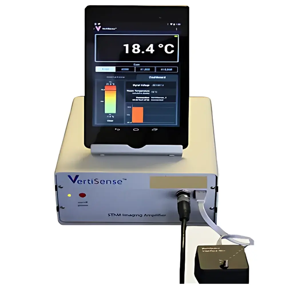
AppNano VertiSense Scanning Thermal Microscopy (SThM) Module for Atomic Force Microscopy
| Brand | AppNano |
|---|---|
| Origin | USA |
| Manufacturer Type | Authorized Distributor |
| Product Category | Imported Instrument |
| Model | VertiSense |
| Instrument Type | Material Science AFM-Compatible SThM Module |
| Primary Function | Nanoscale Thermal Property Mapping (Topography + Thermal Conductivity + Temperature Distribution) |
Overview
The AppNano VertiSense Scanning Thermal Microscopy (SThM) module is a precision-engineered add-on system designed for integration with commercially available atomic force microscopes (AFMs). It operates on the principle of scanning thermal microscopy—where a thermally sensitive, resistive probe (typically a Wollaston wire or doped silicon tip) is scanned across a sample surface in contact or intermittent-contact mode while simultaneously monitoring local temperature, thermal resistance, and heat flux. By coupling topographic feedback with real-time thermal signal acquisition, the VertiSense enables concurrent nanoscale mapping of surface morphology and spatially resolved thermal properties—including local temperature, temperature gradients, relative thermal conductivity, phase transition onset, and qualitative heat capacity variations. This dual-mode capability makes it particularly valuable for characterizing heterogeneous materials where thermal transport behavior deviates significantly from bulk expectations, such as nanowires, carbon nanofiber-reinforced composites, phase-change polymers, and thermoelectric thin films.
Key Features
- AFM-agnostic modular design: Compatible with major platform architectures including Bruker, Keysight, Park Systems, and Asylum Research AFMs via standardized mechanical and electrical interfaces.
- Nanoscale thermal resolution: Achieves localized temperature measurement within ~20 nm lateral resolution under optimized vacuum or ambient conditions—enabled by low-noise Wheatstone bridge readout and active tip temperature stabilization.
- High-temperature probe stability: Utilizes proprietary metallized silicon probes engineered to retain structural integrity and calibration fidelity up to 700 °C, supporting in situ thermal cycling experiments without tip degradation.
- Dual-channel synchronized acquisition: Simultaneously records topographic height data (Z-feedback loop) and thermal contrast signals (voltage drop across heated probe or thermovoltage output), ensuring pixel-aligned thermal–topographic correlation.
- Calibration-ready architecture: Supports traceable calibration using standard reference samples (e.g., Si/SiO₂ step structures, Cr/Au bilayer thermal test patterns) compliant with ISO/IEC 17025 laboratory practices.
Sample Compatibility & Compliance
The VertiSense module accommodates conductive, semiconductive, and insulating samples—including freestanding nanofibers, polymer blends, metal–organic frameworks (MOFs), and epitaxial heterostructures—without requiring conductive coating. Its non-destructive, near-field thermal sensing mechanism avoids beam-induced damage common in electron-beam-based thermal analysis. The system complies with electromagnetic compatibility (EMC) directives per IEC 61326-1 and supports GLP/GMP-aligned workflows through optional audit-trail-enabled software logging. While not a standalone regulatory instrument, its thermal mapping outputs are routinely referenced in ASTM E2581 (Standard Guide for Thermal Analysis of Polymers) and ISO 11357 (Plastics — Differential Scanning Calorimetry) method development contexts.
Software & Data Management
Control and analysis are performed via the VertiSense Control Suite—a cross-platform application built on Qt/C++ with Python API support. The software provides real-time thermal image reconstruction, line-profile extraction along arbitrary paths, differential thermal contrast (DTC) computation, and automated identification of thermal anomalies (e.g., interfacial delamination, filler agglomeration). All raw thermal voltage, Z-piezo, and laser photodiode signals are stored in HDF5 format with embedded metadata (timestamp, setpoint, gain, environmental conditions), enabling reproducible reprocessing and FAIR (Findable, Accessible, Interoperable, Reusable) data handling. Optional 21 CFR Part 11 compliance packages include electronic signature enforcement, user role-based access control, and immutable audit logs for regulated R&D environments.
Applications
- Nanomaterial thermal interface characterization: Quantifying Kapitza resistance at CNT–polymer or graphene–SiO₂ junctions.
- Microelectronic failure analysis: Locating joule-heating hotspots in sub-100 nm interconnects and gate stacks.
- Phase-change memory material screening: Mapping crystallization/melting thresholds in Ge₂Sb₂Te₅ (GST) thin films with <5 K thermal resolution.
- Biopolymer thermal heterogeneity: Detecting localized glass transitions in collagen–hydroxyapatite scaffolds relevant to tissue engineering.
- Thermoelectric film optimization: Correlating Seebeck coefficient gradients with grain boundary distribution in Bi₂Te₃-based nanostructures.
FAQ
Can the VertiSense module be retrofitted onto an existing AFM?
Yes—it requires only standard XYZ scanner access, laser alignment port availability, and analog input/output channels for thermal signal routing. Installation typically completes within one working day with AppNano-certified field application engineers.
Is vacuum operation supported?
The module is rated for operation in ambient air, nitrogen-purged enclosures, and high-vacuum environments down to 10⁻⁶ mbar. Probe thermal drift compensation algorithms are automatically adjusted based on chamber pressure feedback.
What is the minimum detectable temperature difference?
Under optimal signal-to-noise conditions (averaged over 16 frames, 1 Hz scan rate), the system resolves ΔT ≥ 0.3 K at 20 nm lateral scale; absolute temperature accuracy depends on probe calibration and is ±2.5 K traceable to NIST SRM 1470.
Does it support quantitative thermal conductivity mapping?
It provides relative thermal conductivity contrast natively; quantitative conversion requires supplementary modeling (e.g., finite-element simulation of tip–sample heat transfer) and reference measurements on calibrated standards—protocols documented in AppNano Technical Note TN-STHM-04.


