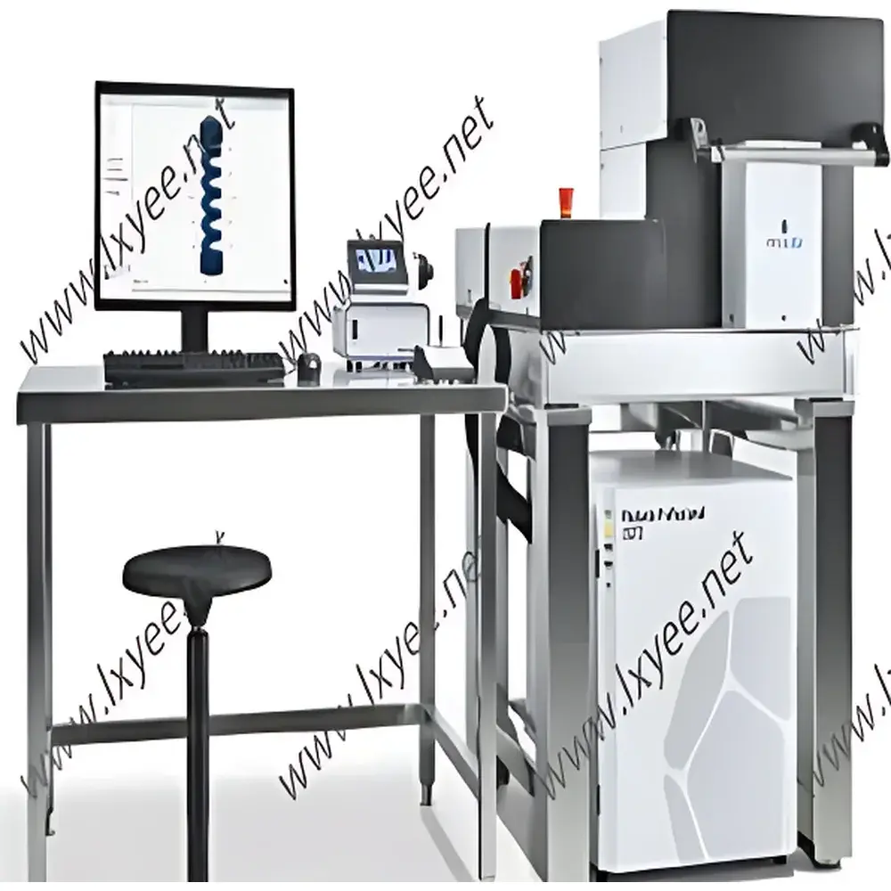

Nanoscribe Photonic Professional GT2 Micro-Nano 3D Printer
| Brand | Nanoscribe |
|---|---|
| Country of Origin | Germany |
| Model | Photonic Professional GT2 |
| Category | Two-Photon Polymerization (TPP) Microfabrication System |
| Automation Level | Fully Automated |
| User Interface | Intuitive Graphical Workflow Environment |
| Compliance Framework | Designed for ISO 14644-1 Class 5 cleanroom integration |
| Software Architecture | Windows-based, FDA 21 CFR Part 11–ready audit trail support (optional configuration) |
Overview
The Nanoscribe Photonic Professional GT2 is a state-of-the-art two-photon polymerization (TPP) micro-nanofabrication system engineered for sub-diffraction-limit 3D structuring of photosensitive materials. Unlike conventional lithographic techniques—including electron beam lithography (EBL), photolithography, or direct laser writing based on single-photon absorption—the GT2 leverages femtosecond pulsed near-infrared lasers to induce highly localized nonlinear photochemical reactions within the focal volume of a high-numerical-aperture objective. This enables true 3D voxel-by-voxel fabrication with isotropic resolution down to <100 nm in lateral and axial dimensions—without requiring masks, development steps, or vacuum environments. The system is purpose-built for research and pilot-scale production in semiconductor device prototyping, photonic integrated circuit (PIC) component fabrication, micro-optics, metamaterials, and bio-inspired microarchitectures.
Key Features
- Fully motorized optical path with automated focus correction and drift compensation, ensuring long-term positional stability during multi-hour printing sequences.
- Integrated galvanometric scanning stage combined with high-precision piezo-driven sample positioning (sub-10 nm repeatability) for seamless stitching across millimeter-scale fields.
- Proprietary IP-L/PGSU/ORMOCER® material compatibility database with validated process parameters for >15 commercially available photoresists.
- Real-time monitoring via synchronized CCD imaging and laser power feedback control to maintain consistent voxel size and crosslinking density.
- Modular vacuum-compatible chamber option for inert-atmosphere processing (N₂ or Ar purging) to suppress oxygen inhibition in acrylate-based resins.
- Pre-calibrated Z-stage and objective lens alignment routines compliant with VDI/VDE 2634 Part 2 standards for traceable dimensional metrology.
Sample Compatibility & Compliance
The Photonic Professional GT2 accommodates standard 100 mm silicon wafers, 4-inch quartz substrates, glass coverslips (thickness 0.13–1.0 mm), and flexible polymer foils (e.g., PET, PI). Substrate clamping uses non-contact electrostatic or vacuum chuck configurations to prevent mechanical deformation. All hardware and software modules are designed to support GLP/GMP-aligned workflows: full electronic lab notebook (ELN) export, user role-based access control, and optional 21 CFR Part 11-compliant digital signature and audit trail functionality. System validation documentation includes IQ/OQ protocols aligned with ISO 9001:2015 and ISO/IEC 17025 requirements for calibration traceability.
Software & Data Management
Nanoscribe’s Quantum X software suite provides an end-to-end workflow—from CAD import (STL, AMF, GDSII via optional converter) to adaptive slicing, path optimization, and real-time print supervision. Slicing algorithms incorporate proximity effect correction and dose modulation mapping to compensate for resin-dependent photon scattering and absorption gradients. Raw print logs (including laser pulse count, galvo position timestamps, and environmental sensor readings) are stored in HDF5 format for post-hoc correlation with SEM/FIB-SEM metrology data. Data export supports ASTM E57.02-compliant point cloud formats and DICOM-RT extensions for biomedical applications.
Applications
- Prototyping of freeform micro-lenses, diffractive optical elements (DOEs), and graded-index (GRIN) waveguides for integrated photonics.
- Fabrication of high-aspect-ratio MEMS components with embedded fluidic channels and movable hinges—fully monolithic, no assembly required.
- Direct-write fabrication of plasmonic nanoantennas, chiral metamaterial unit cells, and photonic bandgap crystals for THz and visible-range devices.
- Microfluidic scaffold fabrication for organ-on-chip platforms, including endothelialized vascular networks with sub-5 µm lumen diameters.
- Maskless fabrication of alignment markers, fiducials, and test structures for process integration into CMOS back-end-of-line (BEOL) workflows.
FAQ
What is the minimum achievable feature size under standard operating conditions?
Typical lateral resolution is 120–180 nm depending on resin formulation, objective NA (1.4–1.6), and laser pulse energy; axial resolution ranges from 250–400 nm. Sub-100 nm features are attainable using optimized ORMOCER® resins and deconvolution-enhanced reconstruction.
Is the system compatible with cleanroom Class 5 environments?
Yes—the GT2 chassis meets ISO 14644-1 Class 5 particulate limits when installed with HEPA-filtered air supply and grounded anti-static enclosures.
Can the system interface with existing semiconductor process control systems?
Via OPC UA and SECS/GEM protocol adapters (available as OEM add-ons), enabling integration into factory automation frameworks such as FabLink XE or Applied Materials Endura platforms.
Does Nanoscribe provide application-specific process recipes?
Yes—validated process kits are supplied for IP-L780, IP-Q, SZ2080, and OrmoComp®, including exposure dose tables, development time profiles, and critical dimension metrology benchmarks.
What level of technical support and service coverage is included?
Standard warranty covers 24 months parts-and-labor; extended service plans include quarterly preventive maintenance, remote diagnostics, and on-site application engineering support for process transfer and DOE optimization.


