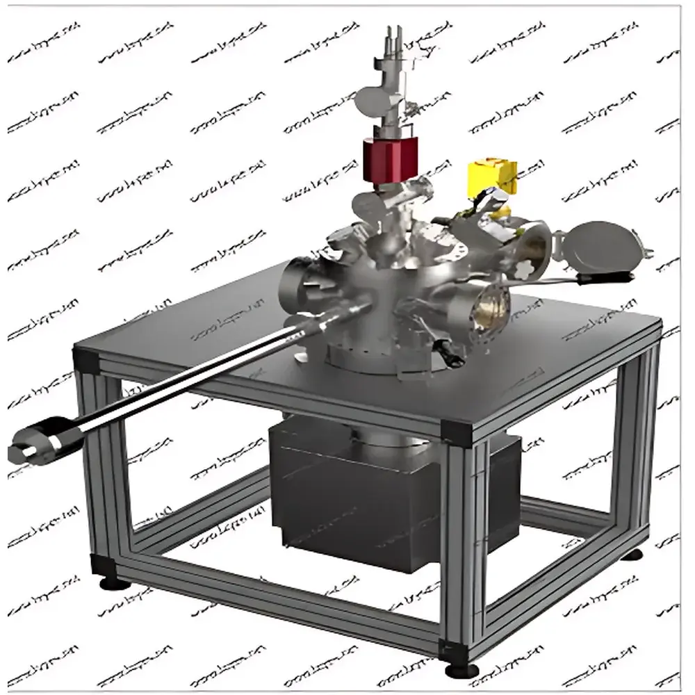

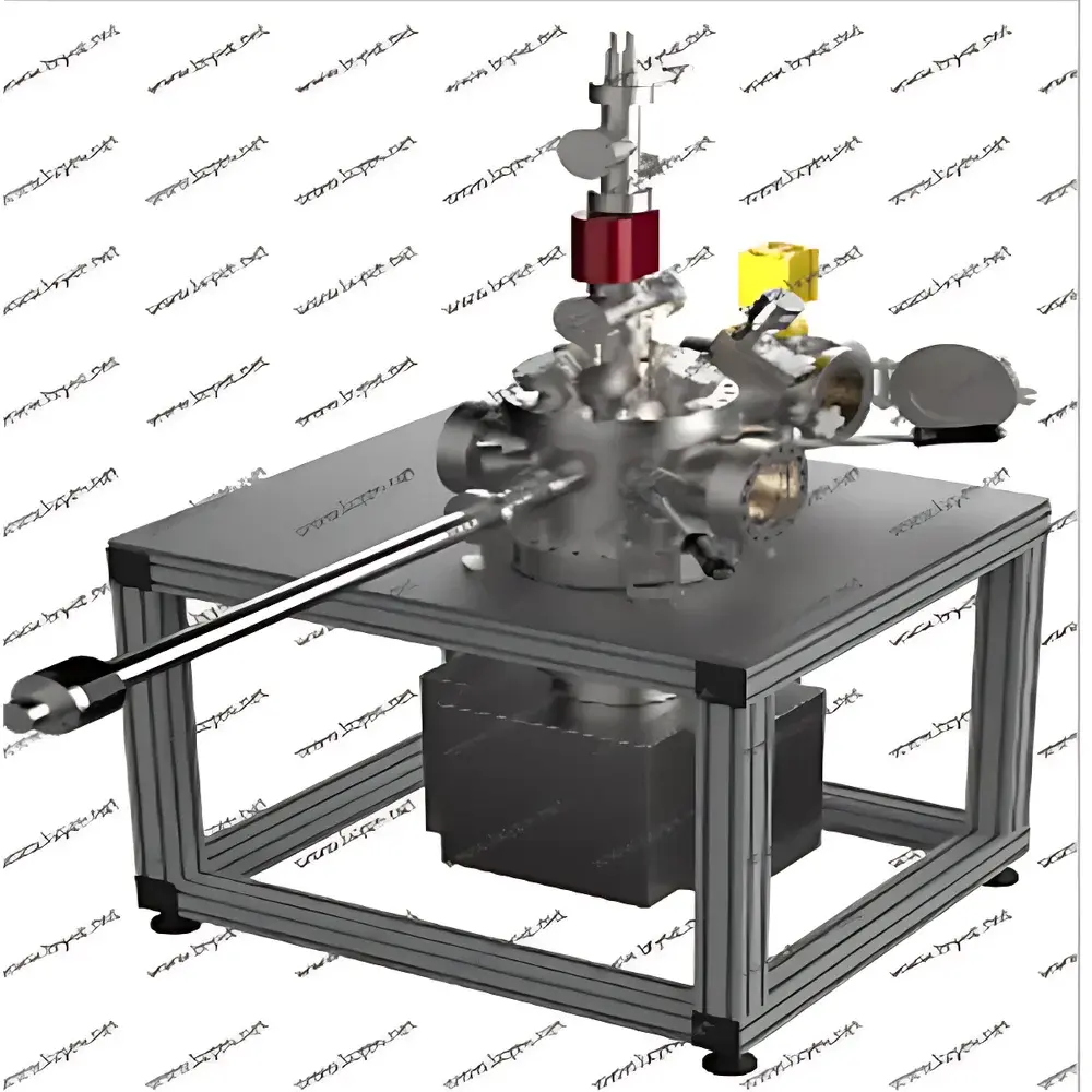
PancanNano ParcanNano Single-Ion Implantation System SII
| Brand | PancanNano |
|---|---|
| Origin | Germany |
| Manufacturer Type | Authorized Distributor |
| Product Category | Imported Equipment |
| Model | SII |
| Product Type | High-Energy Single-Ion Implanter |
| Application Domain | IC & Quantum Device Fabrication |
| Implantation Energy | Custom-configurable per ion species (e.g., 1–100 keV) |
| Ion Dose Range | 1 to 10⁶ ions per site (single-ion counting mode) |
| Wafer Compatibility | Up to 150 mm (6″) substrates, compatible with diced chips and bulk crystals |
| Supported Ions | H⁺, N⁺, O⁺, Si⁺, P⁺, B⁺, As⁺, Te⁺, Ar⁺ (and other singly charged species via optional source modules) |
| Dimensions (L × W × H) | 2.4 m × 1.8 m × 2.2 m (fully shielded vacuum enclosure) |
Overview
The PancanNano ParcanNano Single-Ion Implantation System SII is a high-precision, scanning-probe-based ion implanter engineered for deterministic, sub-10 nm spatial control of individual dopant atoms in solid-state quantum materials. Unlike conventional broad-beam or medium-current implanters governed by statistical distribution and lattice channeling effects, the SII system employs a patented field-emission-driven, tip-integrated nanoscale aperture (<50 nm) combined with real-time ion counting and closed-loop positional feedback. Its core principle relies on electrostatic beam shaping—using conical electric field geometry for ion dilution and collimation, and transverse gate fields to enable single-ion gating at the probe apex—thereby eliminating stochastic straggle and lattice scattering-induced positional uncertainty. Designed specifically for quantum-grade fabrication, the SII delivers traceable, programmable, and repeatable single-ion placement in diamond NV⁻ centers, silicon vacancy arrays, 2D material heterostructures, and epitaxial III–V quantum dots.
Key Features
- Sub-10 nm implantation accuracy: Achieved through integrated atomic-force-microscopy (AFM)-guided positioning and active drift compensation during beam-on dwell.
- Nanoscale ion source architecture: Cantilever-mounted aperture <50 nm in diameter enables diffraction-limited beam confinement and eliminates multi-ion coincidence events.
- Real-time single-ion detection: On-chip microchannel plate (MCP) detector with time-of-flight discrimination ensures verified ion-by-ion delivery with >99.9% counting fidelity.
- Multi-ion compatibility: Modular ion source design supports thermal, plasma, and laser-desorption ionization for H⁺, N⁺, O⁺, Si⁺, P⁺, B⁺, As⁺, Te⁺, Ar⁺, and other singly charged species.
- Ultra-high vacuum environment: Base pressure <5×10⁻⁹ mbar maintained via cryogenic pumping and titanium sublimation, minimizing surface contamination and beam-gas interactions.
- Automated wafer handling: Precision XYZθZ piezo stage with interferometric position feedback and thermal drift stabilization (<0.5 nm/°C).
Sample Compatibility & Compliance
The SII system accommodates planar and non-planar substrates including (100) and (111) oriented diamond, silicon, SiC, h-BN, and GaN wafers up to 150 mm in diameter. It supports both full-wafer processing and localized chip-level implantation under inert gas or UHV conditions. All operational parameters—including ion energy, dose, spot size, and dwell time—are logged with timestamped metadata compliant with ISO/IEC 17025 and GLP audit requirements. The system’s firmware implements hardware-enforced dose limits and interlocked vacuum/beam safety protocols aligned with IEC 61000-6-4 (EMC) and IEC 61010-1 (safety). Optional FDA 21 CFR Part 11-compliant software package provides electronic signature support, audit trail generation, and role-based access control for regulated R&D environments.
Software & Data Management
Control and analysis are performed via PancanNano’s proprietary SII-Studio suite, built on a deterministic real-time Linux kernel. The software features a dual-mode interface: “Quantum Mode” for single-site, ion-counted implantation sequences (including error-corrected re-implantation), and “Array Mode” for scalable patterning of quantum registers (e.g., 8×8 NV arrays with <2 nm pitch uniformity). All raw ion arrival timestamps, stage coordinates, and environmental sensor data (vacuum, temperature, vibration) are stored in HDF5 format with embedded schema definitions. Export modules support direct integration with MATLAB, Python (via PySII API), and commercial TCAD tools (e.g., Synopsys Sentaurus) for post-implant simulation and defect modeling.
Applications
- Creation of deterministic nitrogen-vacancy (NV⁻) centers in isotopically purified diamond for quantum sensing and network nodes.
- Fabrication of atomically precise donor arrays (e.g., phosphorus in silicon) for spin-qubit architectures meeting SiMOS and Kane-model specifications.
- Site-controlled implantation into photonic crystal cavities and plasmonic nanoantennas to engineer single-photon emitters with tailored Purcell enhancement.
- Functionalization of van der Waals heterostructures (e.g., WSe₂/MoS₂) with controlled dopant profiles for tunable valley polarization and optoelectronic switching.
- Development of radiation-hardened test structures for space-grade IC qualification, leveraging traceable single-event effect (SEE) calibration.
FAQ
What vacuum level does the SII system maintain during operation?
The system achieves and sustains a base pressure of ≤5×10⁻⁹ mbar using a combination of cryogenic pumping and titanium sublimation, ensuring minimal beam neutralization and surface adsorption.
Can the SII perform implantation in non-conductive substrates such as diamond or h-BN?
Yes—the system integrates dynamic charge compensation via low-energy electron flood gun synchronized with ion pulse timing, preventing surface charging artifacts across insulating and semi-insulating materials.
Is dose calibration traceable to national standards?
Each instrument undergoes factory calibration against NIST-traceable Faraday cup measurements and single-ion reference standards; calibration certificates are provided with annual recalibration services.
How is beam alignment and focus verified prior to implantation?
A dedicated in-situ beam profiling module uses secondary electron imaging and micro-channel plate intensity mapping to validate spot size, shape, and positional repeatability before sample loading.
Does the system support remote operation and monitoring?
Yes—SII-Studio includes TLS-secured web interface for real-time status monitoring, log retrieval, and emergency stop activation from authorized network endpoints, compliant with ISO/IEC 27001 data governance policies.


