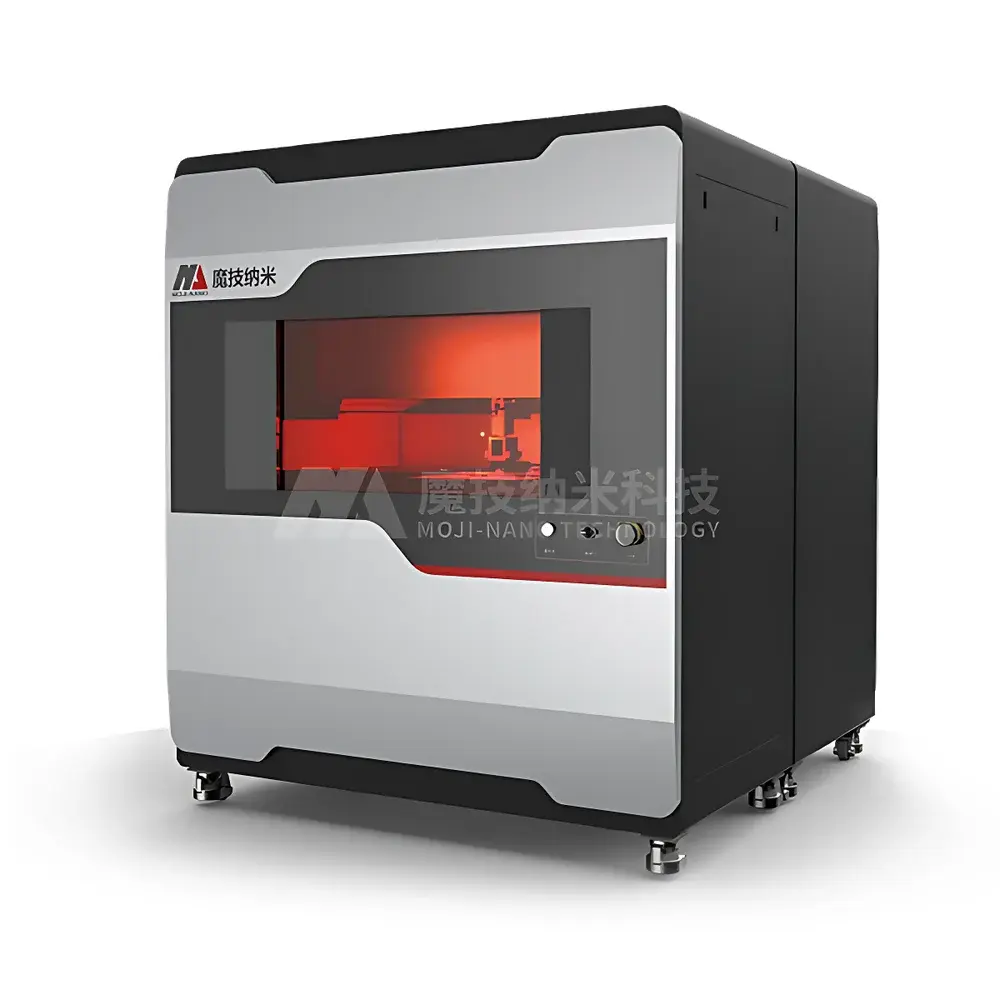
Moji-Nano MJ-Works Ultrafast Laser Micro/Nano Fabrication System
| Brand | Moji-Nano |
|---|---|
| Origin | Shandong, China |
| Manufacturer Type | Original Equipment Manufacturer (OEM) |
| Country of Origin | China |
| Model | MJ-Works |
| Pricing | Available Upon Request |
Overview
The Moji-Nano MJ-Works Ultrafast Laser Micro/Nano Fabrication System is a high-precision, multi-wavelength femtosecond laser platform engineered for three-dimensional micro- and nano-scale material processing. Unlike conventional stereolithography (SLA) or digital light processing (DLP) 3D printers, the MJ-Works employs nonlinear two-photon absorption (TPA) and multiphoton polymerization (MPP) principles—enabled by tightly focused ultrafast pulsed lasers—to achieve true sub-diffraction-limit feature resolution in transparent and non-transparent substrates. Its dual-wavelength femtosecond laser source (typically centered at 515 nm and 1030 nm) allows selective energy deposition across diverse material classes—including fused silica, sapphire, lithium niobate, silicon carbide, stainless steel, titanium alloys, and biocompatible ceramics—without thermal damage or collateral ablation. The system operates as a hybrid additive-subtractive fabrication tool: it supports direct laser writing (DLW) for nanoscale 3D structuring, internal modification of bulk dielectrics, surface texturing, selective laser-induced etching (SLE), and precision micromachining (e.g., drilling, cutting, and selective ablation) with micron-level positional accuracy and long-term process repeatability.
Key Features
- Integrated dual-wavelength femtosecond laser source (515 nm / 1030 nm) with adjustable pulse duration (≤300 fs), repetition rate (1 kHz–5 MHz), and average power control for optimized material interaction
- High-stability XYZ nanopositioning stage with closed-loop piezoelectric actuators and interferometric feedback, enabling ≤50 nm positioning resolution over 100 × 100 mm² scan range
- Automated beam delivery optics with adaptive aberration correction and dynamic focus control for consistent voxel geometry across curved or thick substrates
- Real-time process monitoring via integrated coaxial imaging module (CMOS, 5 MP) and photodiode-based pulse energy monitoring for closed-loop exposure calibration
- Modular vacuum-compatible chamber option for inert-atmosphere processing (N₂ or Ar) to suppress oxidation during metal or ceramic ablation
- Fully automated workflow—from CAD import to path planning, exposure scheduling, and post-processing validation—with G-code and STL compatibility
Sample Compatibility & Compliance
The MJ-Works accommodates substrates up to 150 mm in diameter and 25 mm in thickness, including optical glasses (BK7, SF10), fused quartz, crystalline materials (CaF₂, YAG), semiconductor wafers (Si, GaAs, SiC), metallic foils (Au, Cu, Ni), and bioresorbable polymers (PLA, PCL). All motion control firmware and laser timing modules comply with IEC 61000-6-2/6-4 electromagnetic compatibility standards. The system architecture supports audit-ready operation under GLP and GMP frameworks: software logs all critical parameters (laser fluence, stage coordinates, exposure time, environmental temperature/humidity) with timestamped, tamper-evident records. Optional FDA 21 CFR Part 11-compliant electronic signature and role-based access control modules are available for regulated environments in medical device prototyping and photonics R&D.
Software & Data Management
MJ-Works is controlled by Moji-Nano’s proprietary FabricaSuite™ software—a Windows-based, ISO/IEC 17025-aligned platform supporting both script-driven automation (Python API) and GUI-guided operation. Key capabilities include: automatic lithographic dose calibration using reference gratings; topology-aware slicing for non-planar substrates; real-time voxel size prediction based on material Z-scan data; and native export of metrology-ready files (STL, GDSII, STEP, and ODB++). All raw acquisition data (including laser pulse train metadata and stage trajectory logs) are stored in HDF5 format with embedded SI-unit metadata, ensuring traceability and interoperability with third-party analysis tools (e.g., MATLAB, Python SciPy, MountainsMap®). Backups follow NIST SP 800-88 guidelines, with optional integration into institutional LIMS or ELN systems via RESTful API.
Applications
- Micro-optics & Photonic Integration: Fabrication of freeform microlens arrays, waveguide splitters, photonic crystal cavities, and fiber-tip sensors directly inside single-mode fibers or planar lightwave circuits
- Biomedical Devices: Manufacturing of microfluidic organ-on-chip scaffolds, neural probe electrodes with subcellular feature fidelity, and drug-eluting stent surface textures validated per ISO 10993-5 cytotoxicity protocols
- Semiconductor Packaging: Precision dicing of thin GaN wafers, via formation in Si interposers, and localized stress-engineering of MEMS resonator anchors
- Quantum Technologies: Writing of color center waveguides in diamond (NV⁻, SiV), deterministic placement of nanodiamonds, and fabrication of solid-immersion lenses for spin-photon interfaces
- Aerospace Materials: Surface functionalization of thermal barrier coatings (Y₂O₃-stabilized ZrO₂) to enhance oxidation resistance and promote ceramic matrix composite interfacial bonding
FAQ
What is the minimum achievable feature size in transparent dielectrics?
Under optimized TPA conditions in SZ2080 photoresist or fused silica, the MJ-Works achieves sustained 70 nm lateral and 150 nm axial feature resolution—verified by SEM and AFM traceable to NIST SRM 2053.
Can the system perform simultaneous multi-material processing?
Yes—via sequential laser parameter switching and substrate repositioning within a single automated run; however, true in-situ multi-material deposition requires external material dispensing integration (available as custom OEM module).
Is remote operation supported for facility-shared deployment?
The system includes enterprise-grade TLS 1.3-secured VNC server with hardware-accelerated rendering, enabling low-latency remote control from off-site laboratories while maintaining full metrological traceability.
Does MJ-Works support ISO/ASTM standard-compliant reporting?
FabricaSuite™ generates PDF reports conforming to ISO/IEC 17025 Annex A.2 and ASTM E2911-20 requirements, including uncertainty budgets for dimensional measurements and laser energy stability metrics.
What maintenance intervals are recommended for continuous operation?
Laser source alignment verification every 500 operational hours; stage calibration every 1,000 hours; and full optical path inspection (including objective lens cleaning and collimation check) every 2,000 hours—documented in the included Maintenance Logbook compliant with ISO 9001:2015 clause 7.1.5.
Related Products


