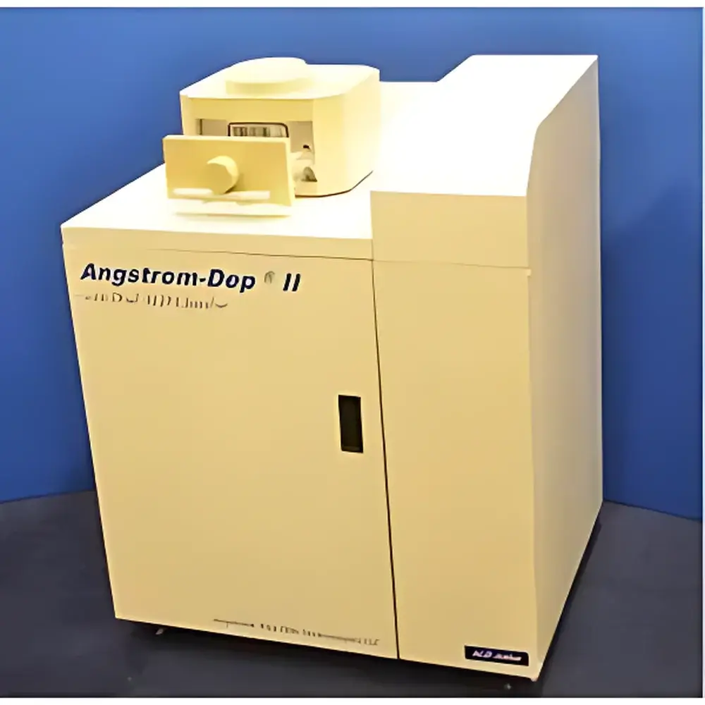
Angstrom Sun Angstrom Dep II Atomic Layer Deposition System
| Brand | Angstrom Sun |
|---|---|
| Origin | USA |
| Model | Angstrom Dep II |
| Substrate Size | 4", 6", 8", or 12" wafers |
| Process Temperature Range | 25–400 °C (optional extended range available) |
| Precursor Channels | 4 standard (upgradable to 6) |
| Uniformity | < 1% (1σ, across full wafer) |
| Footprint | 950 mm × 700 mm (W × D) |
| Cleanroom Compatibility | ISO Class 5 (Class 100) compliant |
| Deposition Modes | Thermal ALD, Plasma-Enhanced ALD (PE-ALD), and Powder ALD capable |
| Weight | Configurable (typical system: ~350 kg) |
Overview
The Angstrom Sun Angstrom Dep II Atomic Layer Deposition (ALD) System is a high-precision, modular thin-film growth platform engineered for research, process development, and pilot-scale semiconductor manufacturing. Based on the self-limiting surface reaction principle, ALD enables atomic-level control of film thickness through sequential, saturative exposure of gaseous precursors—typically metalorganic and oxidizing/nitriding agents—followed by inert purge steps. Each deposition cycle (e.g., pulse A → purge → pulse B → purge) yields a reproducible sub-monolayer increment, ensuring exceptional thickness accuracy, conformality, and stoichiometric fidelity—even over high-aspect-ratio nanostructures, porous substrates, or complex 3D topographies. The Angstrom Dep II implements precise temporal and thermal control over precursor delivery, substrate heating, and chamber pressure, supporting both thermal and plasma-enhanced reaction pathways. Its architecture meets the mechanical, electrical, and environmental requirements for integration into ISO Class 5 cleanrooms and complies with SEMI S2/S8 safety guidelines.
Key Features
- Modular precursor delivery system with four independently controlled, heated mass-flow-controlled gas lines (expandable to six), each equipped with dedicated vaporizer, line heating, and isolation valves to prevent cross-contamination and ensure stable dose reproducibility.
- Uniform resistive heating stage with active temperature feedback control (±0.5 °C stability), supporting operation from ambient to 400 °C; optional high-temperature upgrade available for specialized nitride or carbide processes.
- Integrated RF-powered remote plasma source (13.56 MHz) for PE-ALD mode, enabling low-temperature synthesis of thermally sensitive films (e.g., AlN, TiN) while maintaining high film density and reduced carbon contamination.
- Real-time in-situ monitoring interface compatible with residual gas analyzers (RGA), quartz crystal microbalances (QCM), and optical emission spectroscopy (OES) for process endpoint detection and kinetic analysis.
- Robust stainless-steel vacuum chamber with all-metal seals, base pressure < 1×10⁻⁷ Torr, and integrated turbo-molecular pumping system for rapid pump-down and high-purity processing environments.
- Full I/O integration via industrial Ethernet (EtherCAT) and analog/digital signal ports for synchronization with external tools (e.g., load-lock modules, metrology stations) and factory automation protocols (SECS/GEM).
Sample Compatibility & Compliance
The Angstrom Dep II accommodates standard semiconductor wafers up to 300 mm (12 inch) diameter, as well as non-planar substrates including powders, nanowires, MEMS devices, and porous anodic alumina templates. Custom substrate holders support edge exclusion control and backside helium cooling for thermal management during extended runs. All wetted materials are electropolished 316L stainless steel or ceramic-coated, minimizing metallic contamination and ensuring compatibility with aggressive precursors (e.g., TMA, TEMAHf, NH3, O3). The system conforms to ISO 14644-1 Class 5 (equivalent to Federal Standard 209E Class 100) cleanroom specifications. Electrical safety adheres to UL 61010-1 and IEC 61000-6-2/6-4 EMC standards. Optional validation packages support IQ/OQ documentation aligned with FDA 21 CFR Part 11 and ISO/IEC 17025 requirements for GLP/GMP environments.
Software & Data Management
Control is executed via Angstrom Sun’s proprietary ALD-Studio™ software suite, built on a deterministic real-time operating system (RTOS) with dual-redundant PLC architecture. The GUI provides intuitive recipe editing—including multi-step cycles, conditional branching, and parameter ramping—with full audit trail logging (user actions, setpoints, alarms, sensor readings). All data—including time-stamped process logs, gas flow traces, temperature profiles, and pressure transients—are stored in HDF5 format with embedded metadata (MIAME-compliant). Export options include CSV, MATLAB .mat, and direct SQL database push for integration with enterprise MES or LIMS platforms. Remote diagnostics, firmware updates, and secure SSH access are enabled via TLS 1.2–encrypted network interface, with role-based user permissions (operator, engineer, administrator) and electronic signature support for SOP compliance.
Applications
The Angstrom Dep II supports a broad spectrum of advanced material synthesis critical to next-generation semiconductor, photonic, and biomedical device fabrication. It is routinely deployed for deposition of high-κ dielectrics (Al2O3, HfO2, ZrO2), conductive gate electrodes (TiN, Ru, Ir), diffusion barriers (TaN, WN), piezoelectric layers (AlN, ZnO), transparent conducting oxides (ITO, AZO), OLED encapsulation films (Al2O3), and catalytic nanostructures (Pt, Co3O4). Its PE-ALD capability enables low-temperature (<150 °C) growth of functional coatings on flexible polymer substrates and temperature-sensitive biomaterials. In R&D settings, it facilitates combinatorial library screening, interfacial engineering studies, and atomic-scale heterostructure assembly—particularly where stoichiometry, interfacial sharpness, and defect density must be rigorously controlled per application-specific ASTM F3012, ISO 10477, or JEDEC JESD22-A108 reliability test protocols.
FAQ
What substrate sizes does the Angstrom Dep II support?
Standard configurations accommodate 100 mm (4″), 150 mm (6″), 200 mm (8″), and 300 mm (12″) wafers. Custom chucks for non-standard geometries (e.g., diced dies, fiber arrays, powder boats) are available upon request.
Can the system deposit multi-component or graded films?
Yes. Through synchronized precursor pulsing, variable cycle ratios, and dynamic temperature ramping, the system enables synthesis of ternary oxides (e.g., HfSiOx), doped layers (e.g., Al-doped ZnO), and compositionally graded stacks with sub-nanometer interfacial control.
Is remote plasma operation compatible with ozone or oxygen precursors?
The integrated RF plasma source is fully compatible with O2, N2, NH3, and Ar/O3 mixtures. Plasma dissociation efficiency is tunable via power modulation (0–500 W) and duty cycling to optimize radical density without substrate damage.
How is process repeatability verified across multiple systems?
Each Angstrom Dep II undergoes factory calibration using certified reference wafers (NIST-traceable SiO2/Si standards) and inter-system correlation testing per ASTM E2523. Cross-platform recipe portability is ensured via standardized ALD script syntax and hardware abstraction layer (HAL) drivers.
Does the system support powder ALD for battery or catalyst applications?
Yes. Optional fluidized-bed and rotating drum substrate modules enable uniform coating of micron- to submicron-scale particles (e.g., LiCoO2, Si anodes, MOF powders) with thickness control down to ±0.05 nm per cycle, validated by TEM-EDS depth profiling.
Related Products


