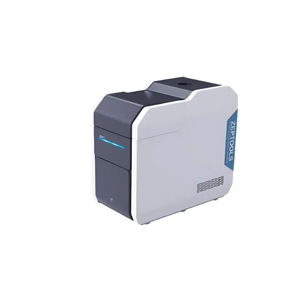
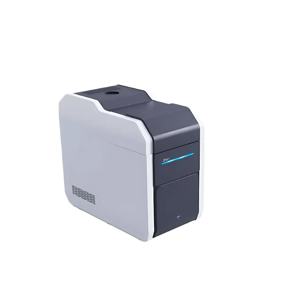
ZEPTOOLS ZEM20 Desktop Scanning Electron Microscope
| Brand | ZEPTOOLS |
|---|---|
| Origin | Anhui, China |
| Manufacturer Type | Direct Manufacturer |
| Instrument Type | Desktop SEM |
| Electron Source | Pre-aligned Tungsten Filament |
| SEM Class | Entry-level Tungsten-Filament SEM |
| Secondary Electron (SE) Resolution | 4 nm |
| Maximum Magnification | 360,000× |
| Accelerating Voltage Range | 3–20 kV (1 kV step adjustment) |
| Backscattered Electron (BSE) Resolution | 4 nm |
| Stage Option | 5-Axis Motorized Stage (Optional) |
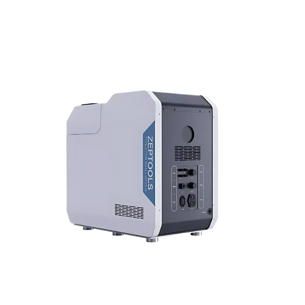
| Chamber Dimensions | 185 mm × 176 mm × 125 mm |
| Vacuum Modes | High Vacuum & Low Vacuum |
| Environmental Suitability | Vibration-isolated design for standard labs/offices/factories |
| Detector Configuration | SE + BSE detectors |
| Optional Upgrades | EDS, Deceleration Mode, In-situ Platforms |
| Filament Upgrade Option | LaB₆ |
Overview
The ZEPTOOLS ZEM20 is a compact, high-performance desktop scanning electron microscope engineered for precision imaging and routine microstructural analysis in academic laboratories, quality control environments, and industrial R&D settings. Based on thermionic emission from a pre-aligned tungsten filament, the ZEM20 delivers stable electron beam performance with minimal alignment intervention. Its dual-mode vacuum system—supporting both high-vacuum (≤1×10⁻³ Pa) and low-vacuum (up to 100 Pa) operation—enables direct observation of non-conductive or hydrated specimens without mandatory metal coating. The instrument employs a fully electromagnetic lens column with integrated condenser optics and fixed aperture configuration, eliminating manual stigmator or objective aperture adjustments during daily use. With an accelerating voltage range tunable from 3 kV to 20 kV in precise 1 kV increments, the ZEM20 balances surface-sensitive low-kV imaging with deeper penetration at higher voltages—critical for multi-layered or bulk material characterization.
Key Features
- 4 nm secondary electron (SE) and backscattered electron (BSE) resolution—validated per ISO 16700:2016 under standard operating conditions.
- 360,000× maximum magnification with real-time digital zoom interpolation and pixel binning for optimized signal-to-noise ratio.
- Vibration-damped mechanical design compliant with ISO 20486-1:2019 for installation in non-dedicated microscopy rooms—including office floors and production facilities.
- Large specimen chamber (185 × 176 × 125 mm) accommodating oversized or irregularly shaped samples, including full wafers, circuit boards, and geological thin sections.
- Deceleration mode (beam landing energy reduction) enables low-voltage surface imaging of beam-sensitive polymers, biological tissues, and uncoated ceramics while preserving topographic contrast.
- Modular architecture supporting seamless integration of optional hardware: energy-dispersive X-ray spectroscopy (EDS) detector, motorized 5-axis stage with tilt/rotation/translation capability, and custom in-situ platforms (e.g., heating, cooling, tensile).
Sample Compatibility & Compliance
The ZEM20 accommodates diverse sample types across materials science, life sciences, geology, and electronics manufacturing. Non-conductive specimens—including polymers, composites, powders, and biological tissues—can be imaged directly in low-vacuum mode or via deceleration-enhanced SE detection. Conductive samples (metals, alloys, doped semiconductors) are routinely analyzed in high-vacuum mode at optimal kV settings. All operational parameters adhere to IEC 61000-6-3 (EMC emissions) and IEC 61000-6-2 (immunity). The system supports GLP-compliant documentation workflows when paired with optional audit-trail-enabled software modules, and meets foundational requirements for ISO/IEC 17025-accredited testing laboratories where SEM-based morphology assessment is included in scope.
Software & Data Management
Acquisition and analysis are managed through ZEPTOOLS’ proprietary SEM Suite v3.x—a Windows-based application offering real-time image acquisition, automated focus/stigmation routines, multi-detector signal mixing (SE/BSE ratio imaging), and calibrated measurement tools traceable to NIST-standard reference grids. Raw image data is stored in TIFF 6.0 format with embedded metadata (kV, WD, dwell time, magnification, detector type). Export options include CSV (for quantitative intensity profiles), JSON (for metadata exchange), and standardized HDF5 containers compatible with open-source analysis frameworks such as HyperSpy and DigitalMicrograph. Software licensing includes remote diagnostics support and biannual firmware updates aligned with CE/UKCA regulatory revisions.
Applications
- Materials characterization: grain boundary mapping in sintered ceramics, fracture surface analysis of metallic alloys, dispersion uniformity assessment in nanocomposites.
- Electronics failure analysis: solder joint integrity, PCB trace delamination, MEMS device inspection, and lithography pattern fidelity verification.
- Life science correlative workflows: cryo-fractured tissue sections, freeze-dried biofilms, and mineralized extracellular matrix visualization.
- Geoscience and mining: clastic grain morphology, porosity quantification in shale cores, and elemental zonation in ore minerals (when coupled with EDS).
- Quality assurance: incoming raw material screening, coating thickness estimation via edge contrast, and defect root-cause identification in injection-molded components.
FAQ
Is the ZEM20 suitable for uncoated biological samples?
Yes—the low-vacuum mode (up to 100 Pa) and deceleration imaging capability allow direct observation of hydrated or insulating biological specimens without sputter coating.
What vacuum level is required for EDS integration?
EDS operation requires high-vacuum conditions (≤5×10⁻⁴ Pa); the ZEM20’s dual-pump system (turbomolecular + rotary vane) achieves this within <90 seconds after chamber venting.
Can the 5-axis stage be retrofitted to existing units?
Yes—ZEM20 systems manufactured after Q3 2022 support field-upgradeable motorized stages via certified service technician deployment and firmware reconfiguration.
Does the system comply with FDA 21 CFR Part 11 for regulated industries?
The base configuration supports electronic signatures and audit trails when deployed with optional Validation Package (VP-ZEM20), enabling compliance in pharmaceutical excipient or medical device QA/QC applications.
What is the typical service interval for the tungsten filament?
Under standard usage (4–6 h/day, 15 kV average), filament lifetime exceeds 150 operating hours; LaB₆ upgrade extends this to >500 h with improved brightness and stability.


