ZOLIX SCS10-Film Spectral Response and Quantum Efficiency Measurement System for Thin-Film Photovoltaic Materials
| Brand | ZOLIX |
|---|---|
| Origin | Beijing, China |
| Manufacturer Type | Direct Manufacturer |
| Product Origin | Domestic (China) |
| Model | SCS10-Film |
| Pricing | Upon Request |
| Spectral Range | 300–1700 nm |
| Wavelength Accuracy | ±0.2 nm (@ 1200 g/mm grating, 500 nm) |
| Scan Interval | 0.1–10 nm (default 10 nm) |
| Bandwidth | 0.1–10 nm (default 5 nm) |
| Light Source | 150 W stabilized xenon lamp (optical stability ≤0.4%) |
| Modulation Frequency | 4–400 Hz |
| Detector | Calibrated Si photodiode |
| DC Sensitivity | 100 nA |
| AC Sensitivity | 2 nV |
| Repeatability | <0.6% (<0.3% from 400–1000 nm) |
| Scan Speed | <1 min per spectral response curve |
| Sample Stage | 156 mm × 156 mm probe station (customizable) |
| max sample area | 300 mm × 300 mm |
| Mapping Resolution | 0.5 mm |
| Mapping Speed | 20 points/s (@ 0.5 mm step) |
| Instrument Dimensions | Host unit: unspecified |
| Sample chamber | unspecified |
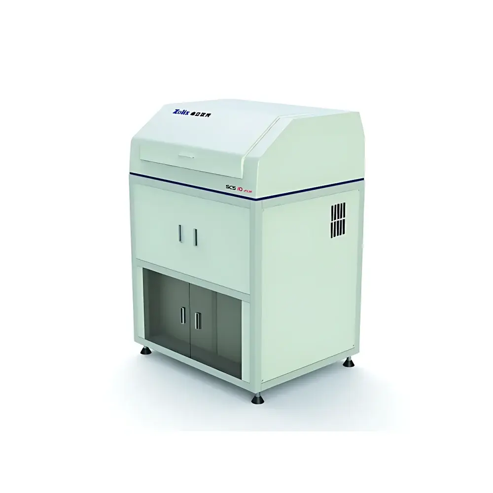
| Control cabinet | 800 mm × 600 mm × 1300 mm |
| Software | Windows 7-based proprietary control & analysis suite with calibration traceability |
Overview
The ZOLIX SCS10-Film Spectral Response and Quantum Efficiency Measurement System is a turnkey optical characterization platform engineered for quantitative evaluation of thin-film photovoltaic (PV) materials and devices. It operates on the principle of monochromatic photocurrent spectroscopy, combining calibrated broadband illumination, high-resolution wavelength selection, and lock-in amplification to determine spectrally resolved photoresponse under controlled bias and illumination conditions. Designed specifically for research, process development, and quality assurance in thin-film solar cell manufacturing, the system supports standardized measurement of external quantum efficiency (EQE), internal quantum efficiency (IQE), spectral responsivity (Rλ), reflectance (Rλ), transmittance (Tλ), and short-circuit current density (Jsc). Its 300–1700 nm spectral coverage accommodates single-junction amorphous silicon (a-Si:H), multi-junction tandem structures (a-Si/μc-Si, a-Si/μc-Si/μc-SiGe), chalcopyrite CIGS, and cadmium telluride (CdTe) absorber layers—enabling direct correlation between optical absorption profiles and charge-carrier generation efficiency.
Key Features
- Integrated turnkey architecture with pre-aligned optical path, eliminating field calibration overhead and minimizing alignment drift during extended operation.
- High-stability 150 W xenon lamp coupled via optical fiber to ensure uniform spectral delivery and thermal decoupling from the sample chamber.
- DSP-controlled triple-grating monochromator enabling precise wavelength selection across UV-VIS-NIR (300–1700 nm), with programmable bandwidth (0.1–10 nm) and auto-switching multi-order suppression filters to eliminate stray light and higher-order diffraction artifacts.
- Dual-mode detection: DC mode for absolute photocurrent quantification and AC lock-in mode (4–400 Hz) for enhanced signal-to-noise ratio in low-light or high-capacitance device measurements.
- Large-format sample chamber accommodating substrates up to 300 mm × 300 mm, with modular probe station (standard 156 mm × 156 mm) and rapid back-contact interface for grounded or floating electrode configurations.
- Simultaneous acquisition of EQE, IQE, Rλ, and Tλ within a single automated sequence—reducing measurement uncertainty associated with sequential repositioning or recalibration.
Sample Compatibility & Compliance
The SCS10-Film system is validated for use with standard and custom thin-film PV architectures, including single-junction, two-terminal (2T) and three-terminal (3T) tandem cells, semi-transparent devices, and textured or patterned absorbers. Sample handling complies with IEC 60904-8 (Photovoltaic devices — Part 8: Measurement of spectral response of a photovoltaic (PV) device) and ASTM E1021 (Standard Test Methods for Spectral Responsivity Measurements of Photovoltaic Devices). Reflectance and transmittance measurements adhere to ISO 9050 (Glass in building — Determination of light transmittance, solar direct transmittance, total solar energy transmittance, ultraviolet transmittance and related properties). The system’s optical calibration traceability follows NIST-traceable reference diodes (e.g., Hamamatsu S1337 series), and all spectral data files include metadata compliant with PV industry reporting conventions (e.g., Jsc integration over AM1.5G spectrum per IEC 60904-3).
Software & Data Management
The system includes a dedicated industrial PC running Windows 7 (64-bit) with ZOLIX’s proprietary measurement and analysis software. The GUI provides real-time spectral preview, multi-parameter synchronization control (bias voltage, modulation frequency, grating position), and automated calibration workflows—including dark-current subtraction, reference diode normalization, and Fresnel-corrected IQE derivation. Data export supports CSV, TXT, and HDF5 formats with embedded metadata (wavelength, intensity, bias, temperature if integrated). Audit trail functionality logs all user actions, parameter changes, and calibration events—supporting GLP-compliant documentation requirements. While not natively 21 CFR Part 11 certified, the software architecture permits integration with third-party electronic lab notebook (ELN) systems for full regulatory traceability in GMP environments.
Applications
- Process optimization of sputtered, co-evaporated, or solution-processed thin-film absorbers (CIGS, CdTe, perovskite precursors).
- Quantitative assessment of interfacial recombination losses via IQE/Rλ comparison across layer stacks.
- Validation of anti-reflection coating performance and front/back contact transparency.
- Mapping of spatial uniformity in large-area modules (e.g., P1–P3 scribe line integrity, shunt resistance distribution).
- Accelerated aging studies correlating spectral degradation modes with encapsulant yellowing or interlayer diffusion.
- Support for interlaboratory round-robin testing under IEA-PVPS Task 12 protocols.
FAQ
What photovoltaic material systems are supported by the SCS10-Film system?
The system is optimized for amorphous silicon (a-Si:H), microcrystalline silicon (μc-Si), CIGS, CdTe, and multi-junction thin-film architectures—including dual- and triple-junction tandems with Ge or SiGe bottom cells.
Can the system measure devices under forward bias or illumination bias?
Yes. The integrated source-measure unit supports programmable DC bias (±10 V, 1 A) and simultaneous illumination bias using an optional white LED or halogen lamp module—enabling Voc-dependent EQE and carrier collection analysis.
Is spectral calibration performed in-house or by the user?
Factory calibration uses NIST-traceable reference photodiodes at discrete wavelengths (300, 400, 500, 600, 700, 800, 900, 1000, 1200, 1400, 1600, 1700 nm). Users may perform periodic verification using supplied calibration standards; full recalibration is available through ZOLIX service centers.
Does the software support automated Jsc calculation from EQE data?
Yes. The software integrates EQE spectra against the AM1.5G reference spectrum (IEC 60904-3) and outputs Jsc values with configurable integration limits and interpolation methods (linear, cubic spline).
What is the minimum detectable photocurrent in AC mode?
At 100 Hz modulation and 1 s time constant, the system achieves a noise floor of ≤2 nV RMS, corresponding to sub-picoampere photocurrent resolution for typical 1 kΩ shunt resistances.


