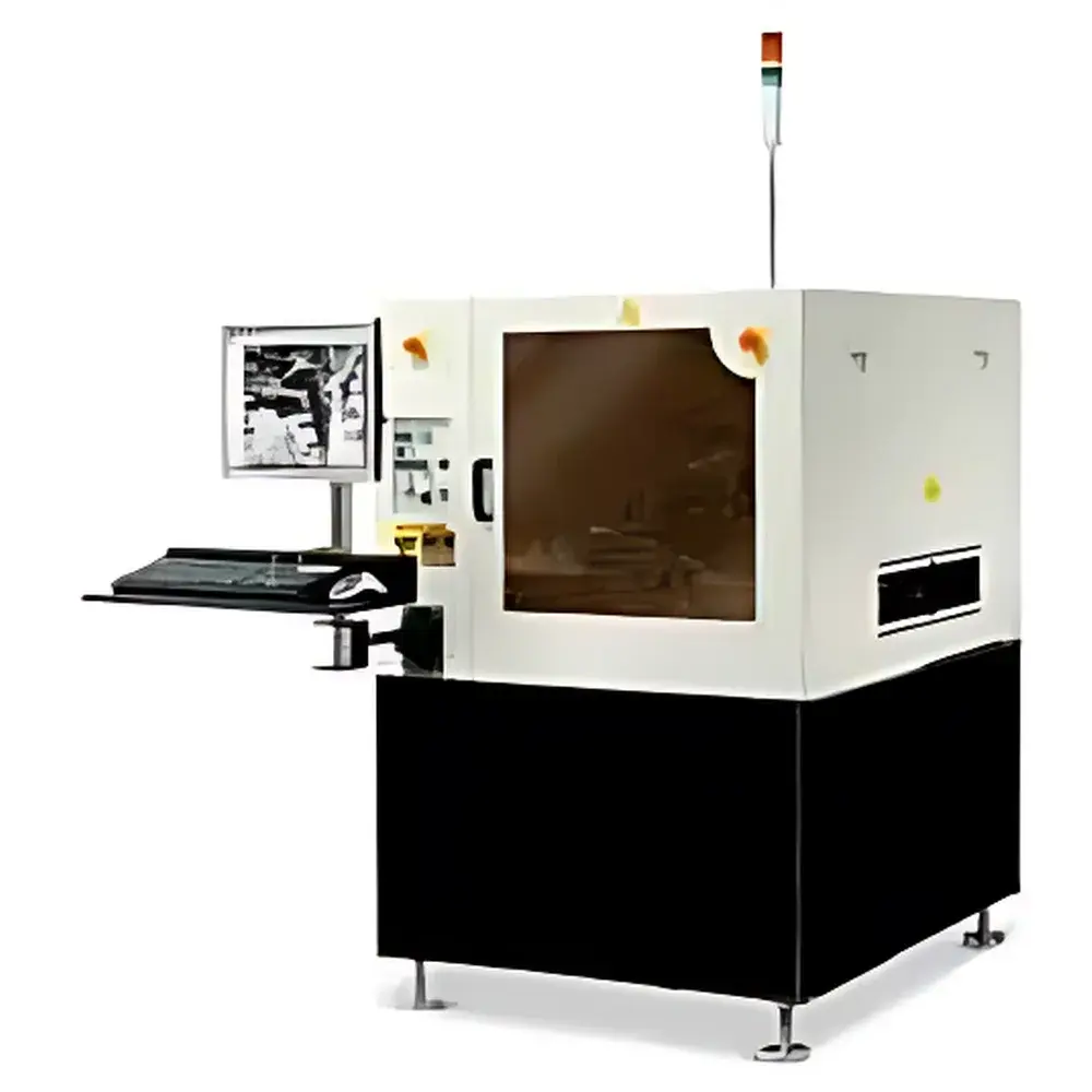
Helios Photoluminescence Imaging System
| Brand | ZOLIX |
|---|---|
| Origin | Beijing, China |
| Manufacturer Type | Original Equipment Manufacturer (OEM) |
| Product Origin | Domestic (China) |
| Model | Helios |
| Pricing | Available Upon Request |
Overview
The Helios Photoluminescence (PL) Imaging System is a high-speed, industrial-grade optical measurement instrument engineered for real-time, non-contact characterization of semiconductor wafers and photovoltaic (PV) cells. Based on the fundamental principle of photoluminescence—where incident photons excite electron-hole pairs in crystalline silicon, and subsequent radiative recombination emits near-infrared (NIR) photons—the Helios system captures spatially resolved PL intensity maps to quantify minority carrier lifetime distribution across the entire wafer surface. This quantitative lifetime imaging enables direct correlation with material quality, defect density, and recombination activity—critical parameters governing solar cell conversion efficiency. Designed specifically for integration into high-throughput PV manufacturing lines, Helios operates as both an inline process monitor and an offline analytical tool, delivering sub-second per-wafer acquisition without compromising signal-to-noise ratio or spatial fidelity.
Key Features
- High-speed full-wafer imaging: Acquires calibrated PL intensity maps in under 1 second per standard 156–210 mm silicon wafer, enabling 100% inspection at production line speeds.
- InGaAs-based NIR detection: Equipped with thermoelectrically cooled InGaAs focal plane array (FPA) sensors optimized for the 900–1700 nm spectral range, ensuring high quantum efficiency and low dark current for robust lifetime quantification.
- Flexible deployment architecture: Supports both conveyor-coupled inline monitoring (with automated trigger synchronization) and benchtop offline analysis modes—compatible with standard wafer handling systems (FOUPs, cassettes, robotic arms).
- Intuitive operator interface: Features a purpose-built graphical user interface (GUI) with pass/fail thresholding, color-coded lifetime heatmaps, statistical process control (SPC) charts, and configurable alarm logic for immediate process deviation detection.
- Robust mechanical design: Engineered for 24/7 operation in cleanroom environments (ISO Class 5–7 compatible), with vibration-damped optical housing, sealed optics path, and modular electronics for field serviceability.
Sample Compatibility & Compliance
The Helios system is validated for use with monocrystalline and multicrystalline silicon wafers (Czochralski and cast ingots), including textured, coated (SiNx, AlOx), and metallized substrates. It supports industry-standard wafer formats from M2 to G12 (156.75 mm to 210 mm) and accommodates thicknesses ranging from 120 µm to 200 µm. Measurement traceability aligns with ASTM F1535-22 (Standard Test Method for Minority Carrier Lifetime of Silicon Wafers by Quasi-Steady-State Photoconductance) and IEC 62788-5-1 (Measurement of minority-carrier lifetime in crystalline silicon). All data acquisition and reporting workflows are structured to support GLP/GMP-aligned documentation requirements, including audit trails, user access controls, and electronic signature readiness.
Software & Data Management
The Helios Control Suite is a Windows-based application built on a modular architecture compliant with FDA 21 CFR Part 11 for electronic records and signatures. It provides real-time image acquisition, lifetime calibration (via reference wafer or built-in LED stability monitoring), spatial noise correction, and pixel-wise τeff calculation using calibrated camera response and excitation uniformity mapping. Export options include TIFF (16-bit), CSV (lifetime matrix + metadata), and PDF reports with SPC summary statistics (Cp/Cpk, yield trend, defect clustering analysis). Data can be streamed via OPC UA or MQTT to MES/SCADA platforms for closed-loop process feedback.
Applications
- Raw material qualification: Automated wafer grading based on bulk lifetime distribution prior to diffusion—enabling segregation of low-lifetime wafers before high-cost processing steps.
- In-line process monitoring: Real-time tracking of lifetime degradation during POCl3 diffusion, PECVD SiNx deposition, and firing—identifying furnace drift, gas contamination, or belt speed anomalies.
- Defect diagnostics: Detection of micro-cracks, edge chipping, grain boundary recombination, and metal impurity precipitation invisible to visual or EL inspection.
- Yield root cause analysis: Correlation of PL hotspots with IV curve outliers, electroluminescence (EL) dark areas, and LID/LeTID degradation kinetics.
FAQ
What excitation source does the Helios system use?
Helios employs a high-uniformity, pulsed 850 nm LED array with adjustable pulse width (1–100 ms) and repetition rate (1–10 Hz), optimized for silicon bandgap excitation while minimizing thermal loading.
Can Helios be integrated with existing factory automation systems?
Yes—Helios supports SECS/GEM protocol over TCP/IP, Modbus TCP, and custom API integration for bidirectional communication with host MES and PLC controllers.
Is calibration required between wafers?
No—system-level calibration is performed during startup using internal reference LEDs and NIST-traceable lifetime standards; no per-wafer recalibration is needed.
Does Helios meet ISO/IEC 17025 requirements for accredited testing labs?
While Helios itself is not a certified calibration standard, its measurement methodology and software audit trail features fully support laboratory accreditation under ISO/IEC 17025:2017 when operated within a documented quality management system.


