Shashin Kagaku High-Precision Microscale Printing System for Organic EL and Touch Panel Fabrication
| Brand | Shashin Kagaku |
|---|---|
| Origin | Japan |
| Manufacturer Type | Authorized Distributor |
| Origin Category | Imported Equipment |
| Model | High-Precision Microscale Printing System |
| Pricing | Available Upon Request |
Overview
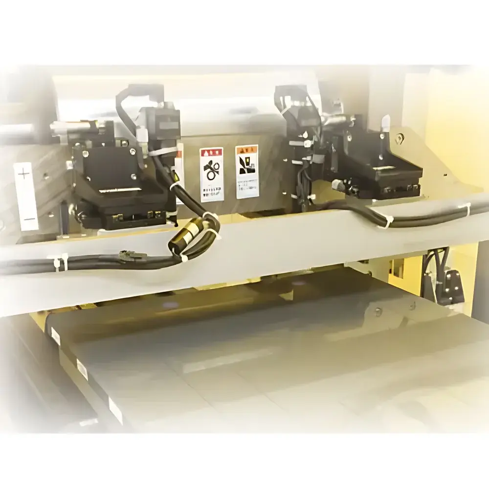
The Shashin Kagaku High-Precision Microscale Printing System is an engineered solution for additive patterning in advanced optoelectronic manufacturing—specifically tailored for organic electroluminescent (OLED/OLET) devices and capacitive touch panel sensor layers. Unlike conventional photolithography or inkjet-based deposition, this system employs a modified offset lithographic principle adapted from semiconductor and flat-panel display equipment design philosophies. It achieves sub-micron registration accuracy and consistent line fidelity through synchronized motion control of substrate stage, printing plate (plate cylinder), and doctor blade assembly. The system operates under ambient or low-temperature thermal conditions (≤120 °C), enabling direct patterning on heat-sensitive flexible substrates—including polyimide (PI), PET, and ultra-thin glass—without requiring vacuum chambers or plasma pretreatment. Its core architecture integrates high-rigidity mechanical frames, air-bearing linear stages, and real-time position/velocity feedback loops to maintain dimensional stability across multi-layer alignment sequences.
Key Features
- Sub-3 µm minimum printable line width with simultaneous multi-width capability—enabling heterogeneous trace geometries within a single pass
- Automated optical registration system with sub-pixel camera alignment and closed-loop positional correction for ≤±0.5 µm overlay accuracy between successive layers
- Dedicated ink compatibility module supporting low-viscosity functional inks (e.g., conductive Ag nanoparticle dispersions, PEDOT:PSS, metal oxide precursors) with shear-thinning rheological profiles
- Independent servo-controlled regulation of impression pressure, web speed, and plate rotation—decoupling mechanical deformation from ink transfer dynamics
- Thermal management subsystem ensuring uniform substrate temperature distribution (<±1.5 °C across 300 mm × 300 mm area) during continuous operation
- Modular tooling interface compliant with standard SEMI E10 carrier handling protocols for integration into cleanroom-based pilot lines
Sample Compatibility & Compliance
The system accommodates rigid (quartz, fused silica, ITO-coated glass) and flexible (PI, PET, PEN) substrates ranging from 100 µm to 1.1 mm thickness and up to 450 mm × 450 mm format. It supports both roll-to-roll (R2R) and sheet-fed configurations via interchangeable stage modules. All motion control firmware and data logging functions comply with ISO 9001:2015 quality management requirements for production equipment. Electrical safety conforms to IEC 61000-6-2 (immunity) and IEC 61000-6-4 (emissions). Optional audit trail and electronic signature modules are available to meet FDA 21 CFR Part 11 and EU Annex 11 expectations for regulated R&D environments.
Software & Data Management
Control is executed via Shashin Kagaku’s proprietary PrintMaster™ v4.2 software suite, running on a deterministic real-time OS. The interface provides full parametric mapping of print parameters—including dwell time per feature, shear rate profile across the meniscus zone, and dynamic registration compensation vectors. All operational logs—including ink viscosity drift alerts, stage encoder deviation reports, and alignment confidence metrics—are timestamped and exportable in CSV or HDF5 formats. Raw image data from alignment cameras may be archived locally or streamed to network-attached storage (NAS) with configurable retention policies. Integration with LabView™ and Python-based analysis pipelines is supported via TCP/IP API and OPC UA server endpoints.
Applications
This system is deployed in university cleanrooms, national research institutes, and corporate R&D centers for prototyping next-generation micro-patterned electronics. Primary use cases include: fabrication of fine-line bus electrodes for in-cell touch sensors; pixel-defining banks in RGB OLED backplanes; transparent conductive mesh structures for large-area capacitive overlays; and printed gate dielectric layers in solution-processed OTFT arrays. Its low-thermal-budget process enables direct integration with temperature-labile encapsulation films and photoresist-free patterning strategies—reducing total cost of ownership relative to vacuum-based alternatives.
FAQ
What substrates can be processed without thermal degradation?
Polyimide (up to 25 µm thickness), PET (≥50 µm), PEN, and ultrathin alkali-free glass (≤100 µm) have been validated at peak process temperatures ≤120 °C.
Is the system compatible with industry-standard CAD data formats?
Yes—Gerber RS-274X, ODB++, and GDSII layouts are directly importable; vector-to-raster conversion includes automatic seam stitching and anti-aliasing optimization for edge fidelity.
How is ink drying integrated into the workflow?
Integrated near-infrared (NIR) flash curing modules (850–1050 nm) provide localized thermal energy delivery; convection ovens and UV LED arrays are available as optional post-print modules.
Can the system be validated for GLP/GMP compliance?
With optional IQ/OQ documentation packages and 21 CFR Part 11-compliant software licensing, the system supports formal validation protocols required for preclinical device development labs.
What maintenance intervals are recommended for sustained sub-micron repeatability?
Laser interferometer calibration of all linear axes every 12 months; ink delivery system purge and filter replacement every 200 operational hours; optical alignment verification prior to each new substrate batch.


