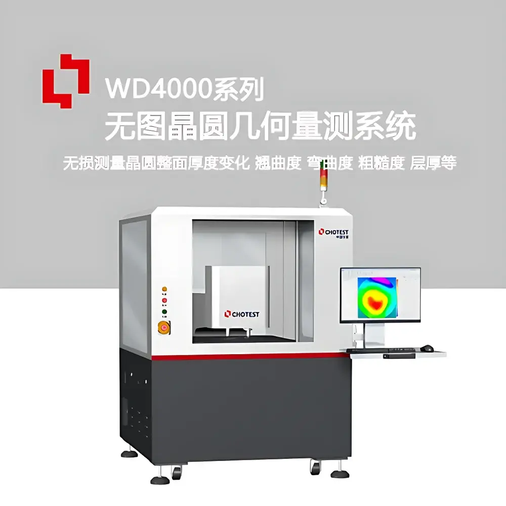
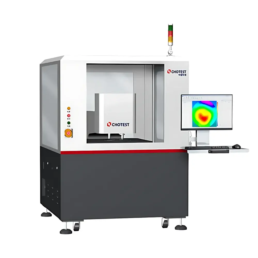
Chotest WD4000 Non-Patterned Semiconductor Wafer Thickness & 3D Topography Metrology System
| Brand | Chotest |
|---|---|
| Origin | Guangdong, China |
| Model | WD4000 |
| Thickness Range | 150 µm – 2000 µm |
| 3D Surface Topography Resolution (Z) | ≤ 0.1 nm |
| Roughness RMS Repeatability | ±0.005 nm |
| Supported Wafer Sizes | 4″, 6″, 8″, 12″ |
| Optical Principle | Spectral Confocal Dual-Side Scanning + White-Light Interferometry (WLI) |
| Max XY Travel | 400 mm × 400 mm |
| Z Travel | 75 mm |
| Scan Modes | Full-map, Cross (‘+’), Custom Multi-point |
| Interferometric Objective Options | 2.5×, 5×, 10×, 20×, 50× |
| Reflectivity Range | 0.05% – 100% |
| Film Thickness Range (IR Interferometry) | 37 µm – 1850 µm (n ≈ 1.5) |
| Minimum Detectable Film Thickness | 0.4 µm |
| Vacuum Chuck | ESD-Safe Perforated Ceramic Vacuum Stage |
Overview
The Chotest WD4000 Non-Patterned Semiconductor Wafer Thickness & 3D Topography Metrology System is an integrated, non-contact optical metrology platform engineered for high-precision characterization of bare (unpatterned) wafers across advanced semiconductor and compound semiconductor manufacturing processes. It combines dual-spectral confocal thickness mapping with white-light interferometric (WLI) surface topography acquisition to simultaneously quantify global geometric parameters—including total thickness variation (TTV), local thickness variation (LTV), bow, warp, site orientation repeatable index (SORI), total indicator reading (TIR), and surface flatness—alongside nanoscale surface texture metrics such as Sa, Sq, Sz, and full ISO 25178–compliant areal roughness parameters. Unlike contact profilometers or single-mode interferometers, the WD4000 employs a synchronized dual-sensor architecture: one spectral confocal head scans the wafer’s front surface while a second precisely time-aligned head measures the back surface, enabling true through-wafer thickness reconstruction without mechanical probing or vacuum-induced deformation. This principle ensures sub-nanometer Z-axis repeatability and eliminates risk of surface scratching, critical for post-CMP, post-grind, or pre-epi inspection of fragile substrates such as GaN, SiC, InP, LiNbO₃, and sapphire.
Key Features
- Integrated dual-mode metrology: Simultaneous spectral confocal thickness mapping and white-light interferometric 3D surface profiling in a single platform.
- High-stability granite-based龙门 (gantry) stage with 400 mm × 400 mm XY travel, 75 mm Z stroke, and 0.1 µm encoder resolution; AC servo direct-drive motors ensure dynamic positioning accuracy under thermal and vibrational load.
- ESD-safe perforated ceramic vacuum chuck compatible with 4″ to 12″ wafers; optimized suction uniformity prevents warpage during measurement.
- Automated multi-point, cross-scan, and full-map programmable measurement routines with real-time path optimization and adaptive focus tracking.
- Dual anti-collision protection: hardware-limit switch interlock + software-defined Z-height guard band to prevent objective–wafer impact during auto-focus or stage motion.
- Motorized turret supporting rapid, repeatable switching among five interferometric objectives (2.5×, 5×, 10×, 20×, 50×) without manual intervention.
- Vision-guided sample alignment: machine vision detects wafer edge and notch/mark features to establish virtual fiducials and auto-correct rotational offset prior to scanning.
Sample Compatibility & Compliance
The WD4000 supports broad material compatibility across legacy and emerging semiconductor substrates—including Si, Ge, GaAs, InP, GaN, SiC, AlN, LiNbO₃, sapphire, fused silica, and glass—with reflectivity tolerance from 0.05% to 100%. Its optical design accommodates both highly reflective polished surfaces and low-reflectivity thin-film-coated wafers without requiring neutral density filters or manual gain adjustment. All thickness and topography measurements comply with ASTM F397 (Standard Test Method for Total Thickness Variation of Silicon Wafers), SEMI MF-1530 (Specification for Wafer Geometry), and ISO 10722:2012 (Geometrical Product Specifications — Surface Texture). The system’s data audit trail, user access control, and electronic signature functionality support compliance with FDA 21 CFR Part 11 and GLP/GMP documentation requirements when configured with optional validation packages.
Software & Data Management
The proprietary MetroStor™ analysis suite provides comprehensive post-processing modules organized into four functional categories: Position Adjustment (e.g., tilt correction, mirroring, plane fitting), Correction (spike removal, spatial filtering, trace repair), Filtering (Gaussian, robust Gaussian, spline, FFT-based spectral filtering), and Feature Extraction (profile/area selection, cross-section slicing, region-of-interest masking). Five analytical engines operate within a unified interface: Geometric Profile Analysis (step height, angle, curvature, straightness, circularity per ISO 1101), Roughness Analysis (full ISO 4287 line-based and ISO 25178 areal parameters), Structural Analysis (void volume, valley depth, peak density), Frequency Analysis (power spectral density, autocorrelation length), and Functional Analysis (material ratio curve, bearing area, plateau ratio). Raw data is stored in vendor-neutral HDF5 format with embedded metadata (timestamp, operator ID, calibration log, environmental conditions), enabling traceability and third-party integration via API.
Applications
- Post-grind/post-polish wafer geometry verification: Quantitative assessment of TTV, bow, and warp prior to epitaxial growth or device fabrication.
- Surface quality monitoring in CMP and dry etch process development: Correlation of Sa/Sq trends with slurry chemistry, pad wear, or endpoint detection algorithms.
- Thin-film stack metrology on unpatterned monitor wafers: Combined IR interferometry (37–1850 µm range) and WLI for multi-layer thickness and interface roughness.
- Substrate qualification for power electronics and RF devices: High-repeatability mapping of SiC and GaN wafer flatness and surface defect density.
- Research-grade 3D morphology studies: Nanoscale characterization of subsurface damage, polishing-induced amorphization, or thermal stress relief patterns.
FAQ
Does the WD4000 require physical contact with the wafer surface during measurement?
No. It uses non-contact spectral confocal and white-light interferometric principles—no stylus, probe, or mechanical force is applied.
Can the system measure wafers with anti-reflective coatings or low-reflectivity films?
Yes. Its adaptive signal processing and wide dynamic range (0.05%–100% reflectivity) enable stable fringe acquisition even on AR-coated or metalized surfaces.
Is full-map thickness mapping supported for 12-inch wafers?
Yes. The 400 mm × 400 mm XY stage and programmable scan path engine support full-die or full-wafer mapping at user-defined sampling densities (e.g., 100 µm grid spacing).
How is measurement traceability maintained for quality audits?
Each measurement includes embedded calibration certificate IDs, environmental sensor logs (temperature/humidity), and full audit trail export compliant with ISO/IEC 17025 and FDA 21 CFR Part 11.
What maintenance is required for long-term stability?
Annual optical recalibration and stage linear scale verification are recommended; no consumables or routine alignment are needed under standard cleanroom operation.


