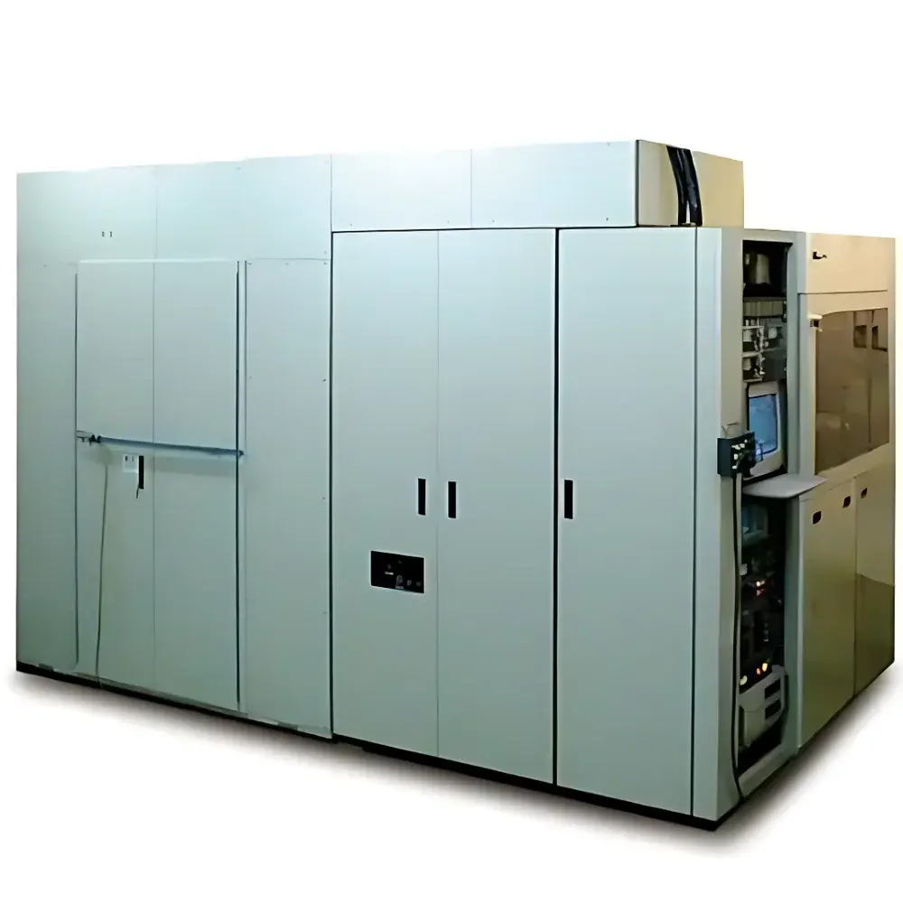
ULVAC KIKO Customized High-Energy Ion Implantation System
| Brand | ULVAC KIKO |
|---|---|
| Origin | Jiangsu, China |
| Manufacturer Type | Authorized Distributor |
| Regional Classification | Domestic (PRC) |
| Model | Customized |
| Product Type | High-Energy Ion Implanter |
| Implant Dose Range | 1×10¹¹ – 1×10¹⁶ atoms/cm² |
| Wafer Sizes Supported | 2", 3", 4", 6", 8" |
| Available Ion Species | B, P, As, Al, S, H, Mg, Si |
| Single-Charge Ion Acceleration Energy | ≥200 keV (with deceleration down to 5 keV) |
| Dose Accuracy | ≤±1.5% |
| Ion Source Configuration | 5-channel solid-source vaporizer (up to 700 °C) |
| Tilt Angles | 0° and 7° (room-temperature stage) |
| Vacuum Performance | Ion Source ≤7×10⁻⁴ Pa |
Overview
The ULVAC KIKO Customized High-Energy Ion Implantation System is a precision-engineered platform designed for controlled dopant introduction into semiconductor substrates via electrostatic acceleration of mass-selected ion beams. Operating on the principle of Coulombic acceleration in high-vacuum environments, the system generates, extracts, analyzes, focuses, and scans monoenergetic ion beams onto wafers with nanoscale spatial uniformity and sub-percent dose reproducibility. It serves as a core process tool in front-end semiconductor fabrication—enabling precise junction formation, threshold voltage tuning, and channel engineering in CMOS, power devices, MEMS, and compound semiconductor structures. Unlike plasma-based doping or diffusion methods, ion implantation offers deterministic depth profiling, minimal thermal budget, and atomic-level compositional control—critical for sub-100 nm node technologies and advanced packaging integration.
Key Features
- High-Energy Single-Charge Ion Acceleration: Capable of accelerating B⁺, P⁺, As⁺, Al⁺, S⁺, H⁺, Mg⁺, and Si⁺ ions to energies ≥200 keV, with integrated deceleration optics enabling fine-tuned final energies from 5 keV to 200 keV—supporting both shallow junctions and deep buried layers.
- Multi-Source Solid-Vaporization Capability: Equipped with five independently controlled vaporizers (operating up to 700 °C), enabling stable, contamination-free generation of ions from solid precursors such as BF₃, PH₃, AsH₃ analogs, Al metal, and elemental Si—eliminating reliance on hazardous gas cylinders.
- Multi-Wafer Compatibility: Fully configurable end station accommodates 2″, 3″, 4″, 6″, and 8″ wafers—including irregular fragments—via programmable platen positioning and beam scanning synchronization.
- Precision Dose Control: Real-time Faraday cup–based beam current monitoring coupled with closed-loop exposure timing ensures dose accuracy within ±1.5% across the full operational range (1×10¹¹ – 1×10¹⁶ atoms/cm²).
- Dual-Angle Implantation Stage: Room-temperature platen supports 0° and 7° tilt for channeling mitigation and angular straggle reduction; high-temperature variant operates at 0° only for in-situ annealing-integrated processes.
- Ultra-High Vacuum Architecture: Segmented vacuum system maintains ≤7×10⁻⁴ Pa in the ion source chamber and ≤7×10⁻⁵ Pa in both beam line and end station—ensuring minimal beam scattering, reduced charge-exchange losses, and long-term source stability.
Sample Compatibility & Compliance
This implanter is validated for use with silicon, silicon carbide (SiC), gallium arsenide (GaAs), and silicon-on-insulator (SOI) substrates. Its mechanical and electrical design conforms to SEMI S2/S8 safety standards and IEC 61000-6-2/6-4 electromagnetic compatibility requirements. The system supports GLP-compliant operation through audit-trail-enabled recipe logging, user-access-controlled parameter locking, and timestamped dose calibration records—facilitating alignment with ISO/IEC 17025 laboratory accreditation frameworks. While not FDA-certified (as it is a capital equipment platform, not a medical device), its process repeatability and metrology traceability are routinely verified per ASTM F1470 (Standard Guide for Ion Implantation Process Control) and JEDEC JESD22-A108 (Reliability Testing for Implanted Devices).
Software & Data Management
The system runs on a real-time Linux-based control platform with deterministic I/O response (<10 ms latency). All implant recipes—including beam energy, dose, tilt angle, scan pattern, vaporizer temperature profiles, and vacuum interlocks—are stored in encrypted SQLite databases with SHA-256 integrity hashing. Data export supports CSV, HDF5, and SEMI E57 formats for integration with factory MES systems (e.g., Applied Materials EnVision, PDF Solutions Exensio). Optional 21 CFR Part 11 compliance package includes electronic signature workflows, role-based access control (RBAC), and immutable audit logs covering all critical parameter changes and maintenance events.
Applications
- CMOS transistor source/drain and well implantation (B, P, As)
- Power device drift region and guard ring formation (Al, S, Mg)
- MEMS piezoresistive layer tailoring (Si, B)
- SiC Schottky barrier optimization (Al, P)
- Hydrogen-induced blistering and smart-cut SOI wafer preparation (H)
- Surface hardening and wear-resistance enhancement of metallic thin films (Si, Al)
FAQ
What ion species can be generated from solid sources?
B, P, As, Al, S, Mg, Si, and H (via metal hydride precursors) are supported using the integrated 5-channel vaporizer array.
Is cluster ion implantation supported?
No—this system is optimized for single-charge monatomic ion beams; cluster or molecular ion capability requires optional RF-driven multicathode source upgrades.
Can the system be retrofitted for 12-inch wafer handling?
Yes—mechanical and software modules for 12″ compatibility are available under ULVAC KIKO’s modular upgrade path (subject to vacuum chamber requalification and beam optics recalibration).
What level of vacuum integrity verification is performed pre-shipment?
Each unit undergoes 72-hour helium leak testing per ASTM E499, with residual gas analysis (RGA) confirming hydrocarbon partial pressure <1×10⁻⁹ Torr before factory acceptance testing.
Does the system include beam profile diagnostics?
Yes—a retractable multi-aperture Faraday cup array and optional slit-scan profiler enable transverse beam current density mapping with ≤0.5 mm spatial resolution.


