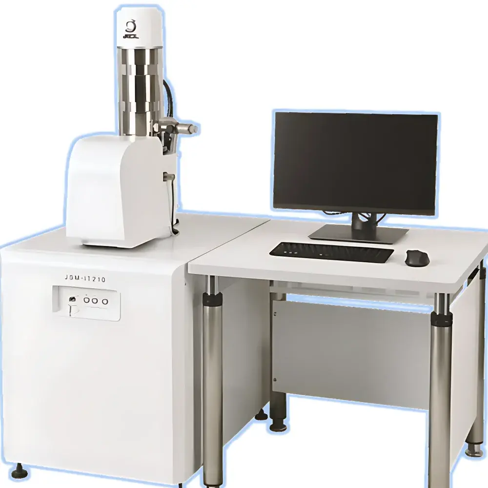
JEOL JSM-IT210 Tungsten-Filament Scanning Electron Microscope
| Brand | JEOL |
|---|---|
| Origin | Japan |
| Model | JSM-IT210 |
| Instrument Type | Floor-standing |
| Electron Source | Tungsten Filament |
| Secondary Electron Resolution | 3 nm @ 30 kV |
| Magnification Range | 5× – 300,000× |
| Accelerating Voltage | 0.5–30 kV |
| Backscattered Electron Resolution | 4 nm (Low Vacuum Mode) |
| Maximum Sample Dimensions | Ø150 mm × 53 mm height |
| Specimen Chamber Expansion Ports | Multiple |
| Stage Type | Motorized 5-Axis Stage |
| Standard Detectors | Everhart-Thornley SE Detector, Solid-State BSE Detector |
Overview
The JEOL JSM-IT210 is a floor-standing tungsten-filament scanning electron microscope engineered for high-reproducibility imaging and routine microstructural analysis in academic, industrial, and quality control laboratories. Introduced in July 2023, it represents the latest evolution of JEOL’s long-established tungsten-filament SEM platform—building directly upon the operational legacy and robust architecture of the widely deployed JSM-6000 series. Unlike field-emission instruments, the JSM-IT210 leverages thermionic emission from a stable, cost-effective tungsten hairpin filament, delivering consistent beam current and extended source lifetime under standard vacuum conditions. Its optical design integrates a digitally controlled condenser lens system with variable focal length and real-time stigmator compensation, enabling precise beam convergence across the full magnification range. The instrument operates on a dual-mode vacuum architecture—high vacuum for optimal secondary electron (SE) contrast and low vacuum for charge-free imaging of non-conductive or hydrated specimens—making it suitable for both metallurgical samples and delicate polymeric or biological materials without mandatory sputter coating.
Key Features
- Digital control architecture with intuitive, icon-driven user interface—designed to minimize operator training time while maintaining full access to acquisition parameters including dwell time, frame averaging, scan speed, and signal mixing.
- Motorized 5-axis specimen stage (X/Y/Z/tilt/rotation) with sub-micron repeatability and programmable coordinate recall—enabling automated multi-site imaging and tilt-series acquisition for qualitative stereoscopic analysis.
- High-sensitivity solid-state backscattered electron (BSE) detector optimized for atomic number (Z)-contrast imaging, coupled with an Everhart-Thornley secondary electron detector for topographic detail at resolutions down to 3 nm at 30 kV.
- Modular chamber design featuring multiple standardized flange ports (CF-63 and CF-100) for integration of optional accessories—including energy-dispersive X-ray spectrometers (EDS), cathodoluminescence (CL) detectors, or environmental SEM (ESEM) gas injection systems.
- Stable high-voltage power supply with fine-step accelerating voltage control (0.1 kV increments between 0.5–30 kV), facilitating landing energy optimization for beam-sensitive samples and surface-sensitive imaging.
Sample Compatibility & Compliance
The JSM-IT210 accommodates specimens up to Ø150 mm in diameter and 53 mm in height—supporting standard SEM stubs, bulk metallographic mounts, printed circuit boards, and fractured mechanical components. Its low-vacuum mode (10–130 Pa) permits direct imaging of insulating ceramics, polymers, composites, and uncoated biological tissues—eliminating charging artifacts without conductive coating. The system complies with IEC 61000-6-3 (EMC emissions) and IEC 61000-6-2 (immunity) standards. For regulated environments, the digital acquisition software supports audit trail logging and user-level permission settings aligned with GLP and GMP documentation requirements. While not inherently 21 CFR Part 11 compliant out-of-the-box, the system architecture allows integration with validated third-party LIMS or ELN platforms via standard DICOM-SEM and TIFF export protocols.
Software & Data Management
Acquisition and processing are managed through JEOL’s proprietary SmartSEM™ software suite—version 2.5 or later—running on a dedicated Windows-based workstation. The software provides real-time image stitching, particle analysis (size, shape, distribution), roughness profiling, and multi-channel signal overlay (SE+BSE+optional EDS). All acquired images include embedded metadata (kV, WD, magnification, detector type, date/time, operator ID), stored in vendor-neutral TIFF format with EXIF-compatible tags. Raw scan data (pixel intensity arrays) can be exported for offline processing in MATLAB, Python (via NumPy), or commercial packages such as ImageJ/Fiji. Remote operation and monitoring are supported via secure RDP or VNC over local network—subject to institutional IT security policies.
Applications
- Metallurgical failure analysis—including fracture surface characterization, inclusion mapping, and intergranular corrosion assessment per ASTM E3, ASTM E1245, and ISO 16700.
- Materials science research—morphological evaluation of catalysts, battery electrode coatings, thin films, and additive-manufactured alloys.
- Electronics quality assurance—cross-sectional inspection of solder joints, wire bond integrity, and die surface defects in semiconductor packaging.
- Geoscience and mineralogy—phase identification via BSE contrast combined with optional EDS, grain boundary delineation in silicates and oxides.
- Life sciences support—low-vacuum imaging of freeze-dried plant tissues, insect cuticles, and dental enamel without carbon/gold sputtering.
FAQ
What vacuum modes does the JSM-IT210 support?
It operates in high vacuum (≤1×10⁻³ Pa) for maximum resolution SE imaging and low vacuum (10–130 Pa) for charge-free observation of non-conductive samples.
Is the tungsten filament user-replaceable?
Yes—the filament cartridge is field-serviceable using JEOL’s standard alignment jig and vacuum lock procedure; typical lifetime exceeds 150 operating hours at 30 kV.
Can the JSM-IT210 be upgraded with EDS?
Absolutely—the chamber includes two dedicated CF-63 ports positioned for optimal take-off angles; compatible with major OEM EDS systems (e.g., Oxford Instruments, Thermo Fisher Scientific, Bruker).
Does it support automated stage navigation?
Yes—the motorized 5-axis stage accepts coordinate lists and supports grid-based area mapping with auto-focus and auto-stigmation at each location.
What is the minimum working distance for optimal resolution?
The standard pole-piece configuration achieves best SE resolution at a working distance of 10 mm; WD can be adjusted from 5 mm to 40 mm depending on sample geometry and signal requirements.


