Atometrics AF Mapping Series X010 Online Thin-Film Thickness Metrology System
| Brand | Atometrics |
|---|---|
| Origin | Guangdong, China |
| Manufacturer Type | Manufacturer |
| Product Category | Domestic |
| Model | AF Mapping Series X010 |
| Pricing | Upon Request |
Overview
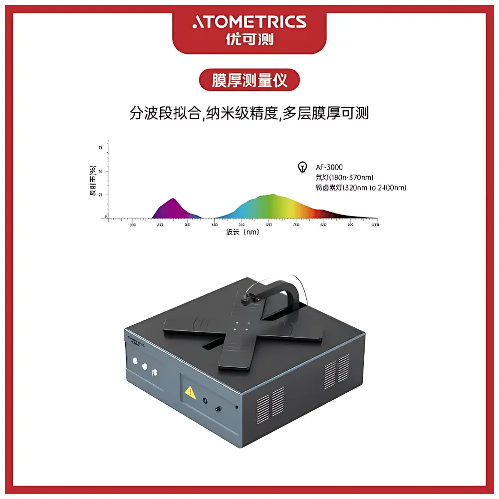
The Atometrics AF Mapping Series X010 is a high-precision, real-time optical metrology system engineered for non-contact, in-line thickness measurement of thin films and multilayer structures during semiconductor, display, photovoltaic, and advanced packaging manufacturing processes. It operates on the principle of spectral reflectometry—analyzing wavelength-dependent interference patterns generated by light reflected from interfaces between layers with differing refractive indices. Unlike conventional single-wavelength or broadband LED-based systems, the X010 integrates dual stabilized light sources: a deuterium lamp (180–370 nm) for deep-UV to near-UV coverage and a tungsten-halogen lamp (320–2400 nm) for extended visible-to-near-IR spectral continuity. This hybrid illumination architecture enables robust characterization across a broad range of material systems—from ultrathin ITO (10 nm) and perovskite layers (18.7 nm) to thick PI films (>30 µm) and bonded glass wafers (3.05 µm)—with sub-angstrom resolution in theoretical modeling and <0.1 s sampling intervals suitable for high-speed roll-to-roll or wafer-level inline monitoring.
Key Features
- Multi-source spectral illumination: Deuterium lamp (180–370 nm) + tungsten-halogen lamp (320–2400 nm) ensures uniform intensity and stable spectral output across UV-VIS-NIR bands
- Segmented spectral fitting algorithm: Patented multi-band curve-fitting engine compensates for systematic dispersion-induced deviations, significantly improving accuracy over traditional global-fit models
- Real-time inline capability: Sampling frequency < 100 ms; compact footprint designed for integration into cleanroom-compatible process tools and conveyor-based production lines
- Multi-layer analysis: Supports up to 10-layer stack modeling—including air gaps, liquid films, rough interfaces, and graded-index layers—without requiring prior knowledge of layer sequence
- Modular configuration options: Available in offline benchtop, inline OEM-integrated, and fully automated wafer-handling variants compatible with 4–12 inch substrates
Sample Compatibility & Compliance
The X010 demonstrates validated performance across diverse film chemistries and substrate types, including transparent conductive oxides (ITO), metal halide perovskites, quantum dot layers, SiO₂ dielectrics, photoresists (e.g., 13.2 µm thick SU-8), polyimide (PI) films, and glass-to-glass bonding interfaces. Measurement repeatability is maintained under varying surface roughness (Ra < 5 nm) and ambient vibration conditions typical of semiconductor fabrication environments. The system complies with ISO/IEC 17025 calibration traceability requirements and supports audit-ready data logging aligned with GLP and GMP documentation standards. While not FDA-cleared as a medical device, its data integrity framework—including user-access controls, electronic signatures, and immutable audit trails—meets foundational expectations for 21 CFR Part 11 compliance in regulated R&D and pilot-scale manufacturing.
Software & Data Management
Control and analysis are performed via Atometrics’ proprietary AF-MAP Studio software, a Windows-based platform featuring intuitive workflow scripting, real-time mapping visualization (2D/3D thickness distribution), and batch report generation compliant with ASTM E2915 and ISO 15630-3 reporting conventions. Raw spectral data is stored in HDF5 format with embedded metadata (wavelength calibration, source status, environmental timestamp). The software supports direct USB 3.0 communication with industrial PLCs and SCADA systems, enabling closed-loop feedback to deposition or etch controllers. Export options include CSV, XML, and PDF reports with configurable pass/fail thresholds and statistical process control (SPC) charting (X-bar/R, Cpk).
Applications
- Semiconductor front-end: Monitoring ALD/CVD/PVD film growth on silicon wafers, including high-k gate stacks and epitaxial layers
- Flat-panel display manufacturing: In-line verification of TFT backplane layers, OLED encapsulation barriers, and touch sensor ITO patterning
- Photovoltaics: Real-time control of perovskite absorber and charge transport layer thicknesses in slot-die coated modules
- Advanced packaging: Thickness uniformity assessment of redistribution layers (RDL), dielectric passivation, and micro-bump underfill
- R&D labs: Quantitative characterization of solution-processed thin films (quantum dots, 2D materials), soft lithography stamps, and microfluidic channel coatings
FAQ
What is the minimum measurable thickness and detection limit for single-layer films?
The system achieves sub-nanometer resolution for optically dense layers (e.g., metals, oxides) and ~1 nm practical lower limit for transparent films such as SiO₂ or polymer layers on reflective substrates, depending on signal-to-noise ratio and optical contrast.
Does the X010 support automatic calibration and drift compensation?
Yes—integrated reference channels monitor lamp intensity stability and detector responsivity in real time; daily auto-calibration routines use certified NIST-traceable silicon wafers with known oxide thicknesses.
Can it measure films on curved or flexible substrates?
Within mechanical alignment tolerance (±2° tilt, ±1 mm Z-height variation), the system accommodates slight curvature and roll-fed flexible films when paired with appropriate stage kinematics and focus-tracking firmware.
Is remote diagnostics and software update supported?
Firmware and software updates are delivered via secure HTTPS; remote diagnostic access requires customer-configured firewall exceptions and authenticated TLS session initiation.
How does the segmented spectral fitting algorithm improve accuracy compared to global fitting?
By partitioning the spectrum into physically meaningful regions (e.g., UV resonance bands for organic layers, NIR interference fringes for thick dielectrics), it mitigates error propagation from dispersion model mismatch—particularly critical for wide-bandgap materials and complex multilayers.

")

