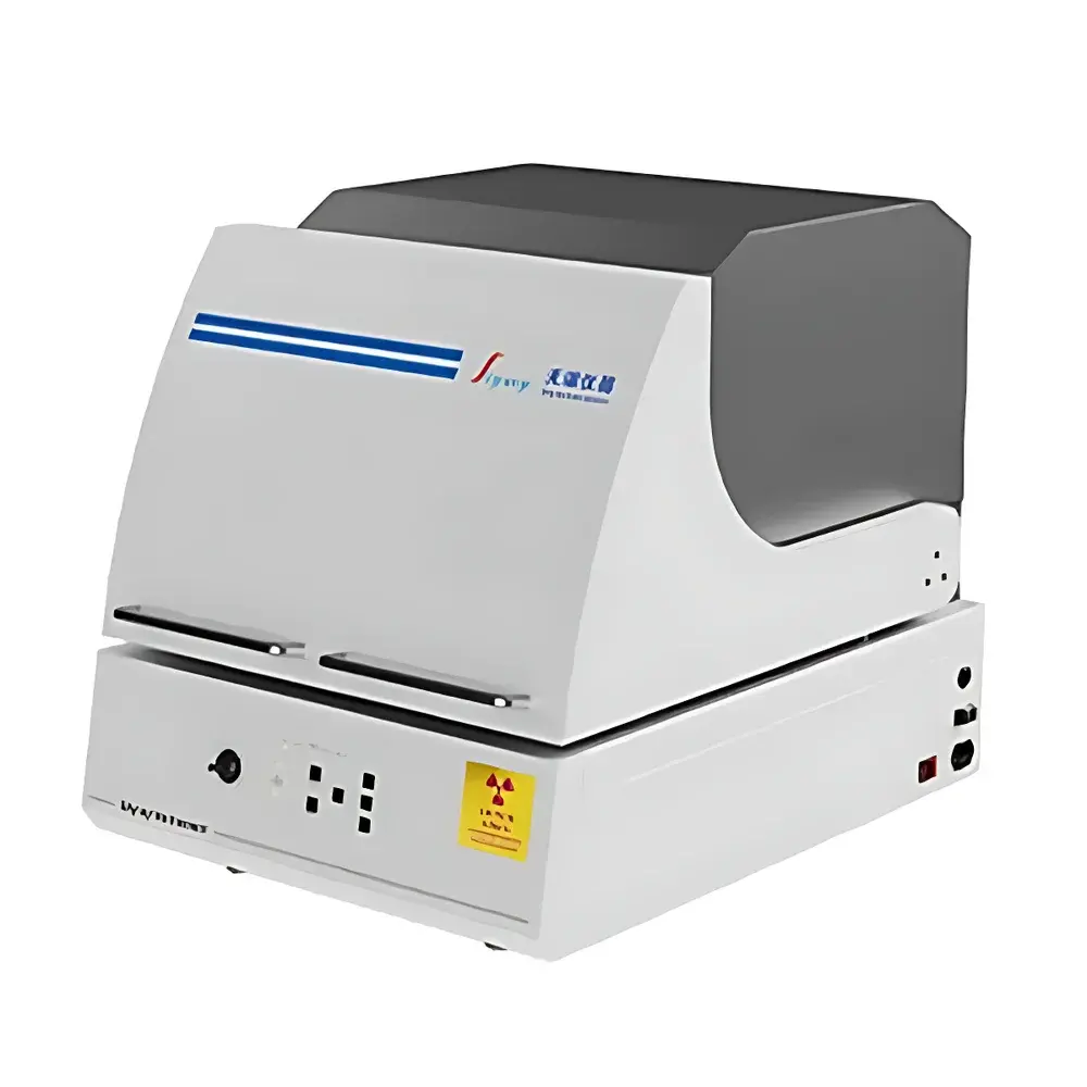
SkyRay EDX-V Energy Dispersive X-Ray Fluorescence Spectrometer for Coating Thickness Measurement and Elemental Analysis
| Brand | SkyRay Instrument |
|---|---|
| Origin | Jiangsu, China |
| Manufacturer Type | Original Equipment Manufacturer (OEM) |
| Country of Origin | China |
| Model | EDX-V |
| Form Factor | Benchtop/Floor-standing |
| Instrument Type | Conventional EDXRF |
| Application Scope | General-purpose coating & thin-film analysis |
| Compliance | ASTM B568, ISO 3497, DIN EN ISO 3497, IPC-4552 (ENIG), IPC-4556 (ENEPIG) |
Overview
The SkyRay EDX-V is a benchtop/floor-standing energy dispersive X-ray fluorescence (EDXRF) spectrometer engineered specifically for non-destructive coating thickness measurement and elemental composition analysis of ultra-thin and multi-layered metallic films. Leveraging over three decades of applied XRF metrology expertise, the instrument implements a proprietary multi-capillary X-ray optics system—designed to concentrate primary X-ray photons onto sub-100 µm sample areas with exceptional spatial resolution and photon flux density. Unlike conventional collimated or polycapillary systems, the EDX-V’s multi-channel capillary optic delivers focused beam intensities enhanced by 10³–10⁴× relative to standard metal collimators, enabling reliable quantification of nanoscale coatings—including Au layers as thin as 2 nm and Pd layers ≤30 nm—without matrix interference or signal saturation. The system operates on fundamental parameter (FP)-based quantification algorithms, calibrated against certified reference materials traceable to NIST and BAM standards, ensuring measurement repeatability <1.5% RSD for homogeneous single-layer deposits under controlled environmental conditions.
Key Features
- Multi-capillary X-ray focusing optics with selectable focal spot diameters (10–50 µm), optimized for micro-area analysis of semiconductor interconnects, lead frames, PCB vias, and wafer-level metallization.
- Dual-camera imaging system: wide-field panoramic camera (10× magnification) for rapid sample navigation + high-resolution micro-camera (5 µm pixel resolution) for precise region-of-interest (ROI) selection and alignment verification.
- High-precision XYZ motorized stage (±0.5 µm positioning repeatability) integrated with dual coaxial laser crosshairs for real-time visual registration and automated multi-point mapping.
- Optimized excitation geometry with ultra-short source-to-sample distance (<3 mm), minimizing air absorption losses and maximizing low-energy X-ray detection efficiency (e.g., for Ni, Cu, Sn, Ag L-lines).
- Si-PIN or SDD detector options (optional), offering count rate capability up to 100,000 cps with energy resolution ≤145 eV at Mn Kα (5.9 keV), supporting high-throughput batch analysis in QC environments.
Sample Compatibility & Compliance
The EDX-V accommodates flat, curved, or irregularly shaped substrates up to Ø150 mm × 30 mm height, including bare wafers, diced dies, connector pins, and flex circuits. Its open-stage design supports both standard sample holders and custom fixtures for inline integration. Analytical protocols are fully compliant with international standards governing electroless and electrolytic plating quality control: ASTM B568 (XRF coating thickness), ISO 3497 (metallic coatings on metallic substrates), IPC-4552A (ENIG—electroless nickel immersion gold), and IPC-4556A (ENEPIG—electroless nickel electroless palladium immersion gold). Data acquisition and reporting modules support audit-ready documentation aligned with GLP and GMP requirements, including electronic signatures, version-controlled method files, and 21 CFR Part 11–compliant audit trails (when configured with optional software license).
Software & Data Management
Controlled via SkyRay’s proprietary QuantMaster™ v5.2 software, the EDX-V provides intuitive workflow management—from method setup and calibration curve generation to automated report export (PDF/Excel/CSV). The software embeds FP-based matrix correction models for multi-layer systems (up to 5 layers), substrate interference compensation, and spectral deconvolution using iterative least-squares fitting. All raw spectra, processed results, instrument parameters, and user actions are timestamped and stored in an encrypted SQLite database. Batch processing mode enables unattended operation across hundreds of predefined positions; results are exportable to LIMS via ODBC or direct API integration. Optional cloud synchronization allows secure remote monitoring and centralized data archiving compliant with ISO/IEC 27001 information security frameworks.
Applications
- Quantitative thickness and composition analysis of functional plating stacks in advanced packaging (e.g., Ni/Pd/Au on Cu pillars, SnAg on solder bumps).
- In-process verification of ENIG and ENEPIG finishes on PCBs and IC substrates per IPC-A-600 and J-STD-003.
- Failure analysis of delamination, interdiffusion, or oxidation in multi-metallic thin films (e.g., TiW/Cu, TaN/Cu, Cr/Au).
- QC screening of precious metal usage efficiency in connector plating lines to optimize material cost without compromising solderability or corrosion resistance.
- Research-grade characterization of novel alloy coatings (e.g., CoWP, NiMoP) for barrier layer development in 3D NAND and logic nodes.
FAQ
Does the EDX-V require vacuum or helium purge for light element analysis?
No—its optimized low-energy response enables reliable detection of elements from Na (11) to U (92) in air; optional He flush upgrade extends sensitivity down to F (9) for specialized applications.
Can it measure coatings on non-conductive substrates such as ceramics or plastics?
Yes—the instrument supports dielectric substrates via charge neutralization mode and matrix-matched calibration; performance validated per ISO 3497 Annex D for insulating bases.
Is method transfer possible between different EDX-V units?
Yes—QuantMaster™ supports standardized method templates with embedded calibration coefficients, ensuring consistent results across distributed manufacturing sites.
What maintenance is required for the multi-capillary optic?
The capillary assembly is sealed and maintenance-free under normal operating conditions; periodic verification using certified thickness standards (e.g., NIST SRM 2136) is recommended every 6 months.
Does the system support automated pass/fail decision logic based on specification limits?
Yes—user-defined tolerance windows trigger color-coded alerts and auto-generate compliance reports compatible with PPAP and APQP documentation workflows.