Applytest NMM-1020 Portable Nanoscale Eddy Current Thickness Gauge
| Brand | Applytest |
|---|---|
| Model | NMM-1020 |
| Measurement Principle | Eddy Current |
| Power Supply | Rechargeable Lithium Battery (20 h runtime) |
| Minimum Sample Size | 150 × 150 mm (flat) |
| Active Measurement Area | Ø40 mm |
| Surface Compatibility | Flat and Curved Substrates (custom calibration profiles supported) |
| Measurement Modes | Contact and Non-Contact (non-contact requires optional probe holder) |
| Connectivity | Bluetooth (optional) |
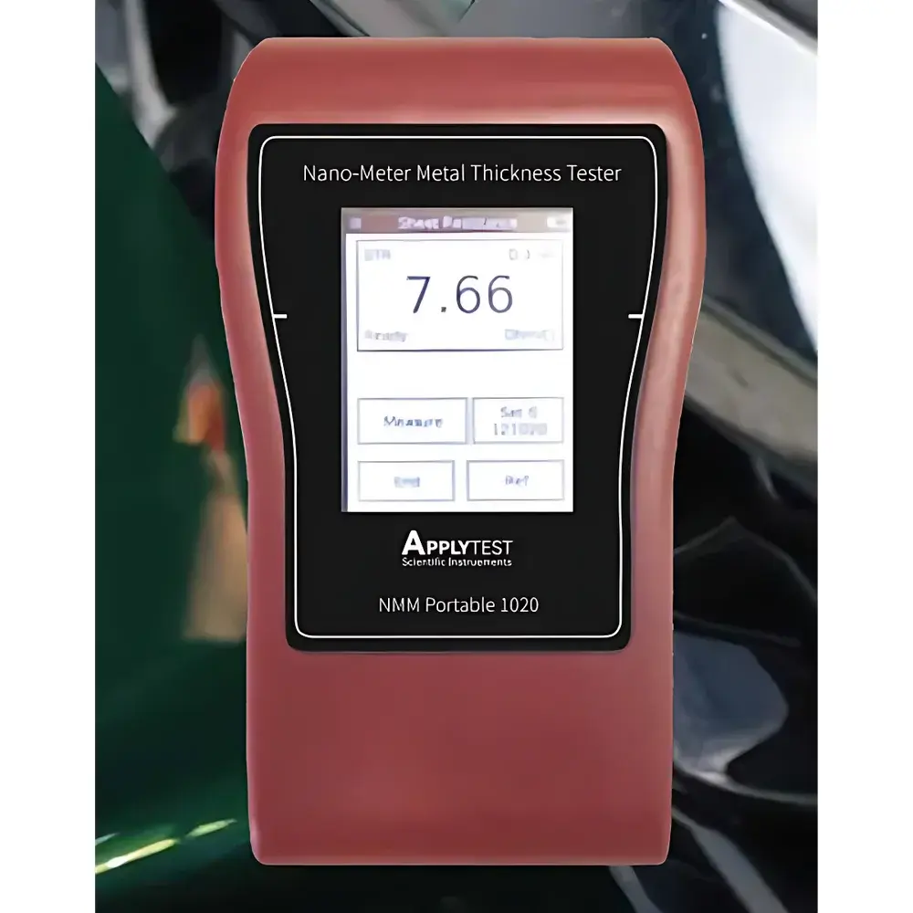
| Display | Integrated Touchscreen Interface |
| Compliance | Designed for ISO 2360, ASTM B244, and IEC 61000-4-3 compliant operation |
| Software | On-device measurement management with export to CSV/Excel |
| Key Measurables | Al (5–540 nm), In (24–2700 nm), Cr (24–2600 nm), Ti (102–11080 nm), Cu (3–340 nm), Ag (3–310 nm), Sn (21–2300 nm), Ni (12–1280 nm) |
Overview
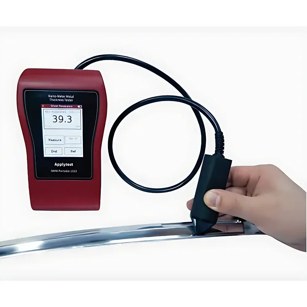
The Applytest NMM-1020 is a handheld, battery-powered eddy current thickness gauge engineered for nanoscale metrology of conductive metallic coatings on non-conductive or semi-conductive substrates. It operates on the principle of high-frequency electromagnetic induction: a coil-driven alternating magnetic field generates eddy currents in the conductive layer; the resulting impedance shift—modulated by coating thickness, conductivity, and substrate permittivity—is quantified via precision analog signal conditioning and real-time digital signal processing. This method enables non-destructive, sub-10-nm resolution thickness assessment without physical contact (when equipped with optional standoff probe mount), making it suitable for quality control in semiconductor packaging, optical thin-film manufacturing, flexible electronics, and advanced packaging R&D. The instrument is calibrated traceably to NIST-traceable reference standards and conforms to the fundamental physical assumptions underlying ISO 2360 (non-magnetic coatings on non-ferrous substrates) and ASTM B244 (standard test method for measurement of thickness of anodic coatings on aluminum).
Key Features
- True nanoscale resolution: Capable of resolving metal layer thicknesses as low as 3 nm (e.g., Cu, Ag) with high repeatability (< ±0.8 nm typical standard deviation under controlled lab conditions)
- Dual-mode operation: Supports both contact mode (probe directly coupled to surface) and non-contact mode (with calibrated air-gap compensation using optional probe holder)
- Adaptive surface compensation: Proprietary algorithm dynamically corrects for dielectric interference from surface contaminants or protective layers (e.g., silicone oil, photoresist residues, anti-static films)
- Curved-surface metrology: User-configurable calibration archives store geometry-specific correction factors for convex/concave substrates (radius range: 25 mm – ∞), eliminating curvature-induced systematic bias
- Integrated touchscreen interface: 5.7-inch capacitive display with intuitive icon-driven workflow; no external PC required for basic measurements or pass/fail thresholding
- Field-deployable architecture: IP54-rated enclosure, 20-hour continuous operation on single lithium-ion charge, and shock-absorbing rubberized housing for industrial environments
Sample Compatibility & Compliance
The NMM-1020 is validated for use on planar and gently curved substrates including polymers (PET, PI, PC), fused silica, borosilicate glass, silicon wafers, and ceramic carriers. Minimum recommended sample footprint is 150 × 150 mm for flat specimens to ensure stable electromagnetic boundary conditions; smaller samples may be measured using edge-compensated calibration protocols (documented in user manual Annex C). All factory calibrations are performed per ISO/IEC 17025-accredited procedures. The device supports audit-ready data logging compliant with GLP and GMP requirements, including timestamped measurement records, operator ID fields, and firmware version tracking—enabling full traceability for FDA 21 CFR Part 11-aligned workflows when paired with optional desktop software.
Software & Data Management
Onboard firmware includes embedded measurement database (up to 10,000 records), statistical process control (SPC) tools (X̄–R charts, Cp/Cpk calculation), and configurable alarm thresholds. Export options include USB-C mass storage mode and optional Bluetooth 5.0 wireless transfer to Windows/macOS applications. The companion Applytest Thickness Suite (v3.2+) provides advanced features: multi-layer stack modeling (for bilayer systems such as Ti/Cu on SiO₂), batch report generation (PDF/CSV), and integration with LIMS via RESTful API. All exported datasets contain metadata headers compliant with ASTM E1447 for materials testing data interchange.
Applications
- Monitoring sputtered or evaporated metal films in MEMS fabrication lines
- In-line QC of metallization on OLED encapsulation barriers
- Verification of seed layer uniformity prior to electroplating in advanced packaging
- R&D characterization of ultra-thin barrier coatings (e.g., Al₂O₃/TiN stacks) on flexible substrates
- Failure analysis of delamination-prone interfaces in heterogeneous bonding processes
- Calibration validation of XRF and ellipsometry instruments in metrology labs
FAQ
Does the NMM-1020 require annual recalibration?
Yes—annual recalibration against certified reference standards is recommended per ISO/IEC 17025 guidelines; calibration certificates include uncertainty budgets and traceability statements.
Can it measure multilayer metal stacks (e.g., Ti/Cu/Ni)?
No—the NMM-1020 measures total conductive layer thickness only. For individual layer resolution in stacks, complementary techniques such as XPS or TEM are required.
Is probe replacement user-serviceable?
Yes—field-replaceable probe modules are available with pre-characterized frequency response curves; each module ships with its own calibration certificate.
What environmental conditions affect measurement stability?
Ambient temperature fluctuations > ±2 °C/min or relative humidity > 85 % RH may induce drift; built-in thermal compensation mitigates this up to ±10 °C/h change rate.
How is measurement uncertainty determined for a given material?
Uncertainty is derived from Type A (statistical repeatability across ≥10 readings) and Type B (calibration standard uncertainty, probe alignment error, substrate conductivity tolerance) components per GUM (JCGM 100:2008).


