UV-Coated Image Sensor SPE by Luqi Technology
| Brand | Luqi Technology |
|---|---|
| Origin | Anhui, China |
| Manufacturer Type | OEM/ODM Manufacturer |
| Origin Category | Domestic (China) |
| Model | SPE |
| Pricing | Available Upon Request |
Overview
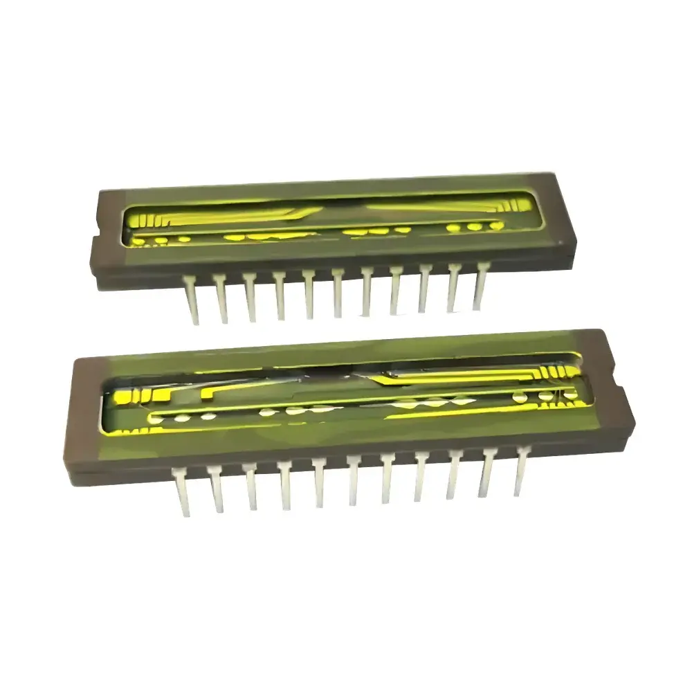
The UV-Coated Image Sensor SPE is a specialized optical sensing component engineered for enhanced quantum efficiency in the deep ultraviolet (DUV) spectral range. Unlike standard silicon-based image sensors—whose native responsivity drops sharply below 350 nm due to strong surface recombination and oxide absorption—the SPE sensor integrates a proprietary vacuum-deposited fluorescent conversion coating directly onto the photosensitive surface. This coating absorbs incident photons in the 200–300 nm band and down-converts them via photoluminescence into longer-wavelength visible photons (typically 400–550 nm), which are efficiently detected by the underlying CMOS or CCD pixel array. The architecture preserves the original sensor’s spatial resolution, readout speed, and dynamic range while significantly extending functional sensitivity into the UV-C and UV-B regions. It is not a standalone imaging camera but a drop-in replacement sensor module intended for integration into custom optical systems, spectrometers, UV inspection platforms, and laboratory-grade fluorescence detection setups.
Key Features
- UV-selective spectral enhancement: Fluorescent thin-film coating optimized for 200–300 nm excitation, with peak quantum efficiency improvement ≥20% relative to uncoated baseline under identical irradiance conditions (measured using calibrated Hg-Ar lamp source)
- High thermal and operational stability: Coating adhesion validated per ISO 2409 (cross-cut test) and humidity resistance tested per IEC 60068-2-78 (85% RH, 85°C, 1000 h)
- Preserved sensor integrity: No degradation of dark current, full-well capacity, or pixel uniformity post-coating; compatible with standard bump-bonding and wire-bonding assembly processes
- Customizable substrate options: Available on monochrome global-shutter CMOS imagers (e.g., Sony IMX series derivatives) or scientific-grade interline-transfer CCDs upon request
- Low outgassing design: Coating materials selected and processed under Class 100 cleanroom conditions to meet UHV-compatible requirements for vacuum-integrated optical benches
Sample Compatibility & Compliance
The SPE sensor is designed for integration into optomechanical systems where UV illumination is delivered via quartz-transmissive optics (e.g., fused silica lenses, MgF₂ windows) and collimated beam paths. It maintains compatibility with standard C-mount or M42 mechanical interfaces, and electrical pinouts conform to industry-standard LVDS or SLVS-EC protocols. While not certified as an end-product medical or aerospace device, the sensor’s manufacturing process adheres to ISO 9001:2015 quality management principles. Material declarations comply with RoHS Directive 2011/65/EU and REACH Annex XVII restrictions. For regulated applications—including UV-curable process monitoring in GMP-compliant pharmaceutical manufacturing—the sensor may serve as a critical subsystem when embedded within a fully validated instrument architecture meeting FDA 21 CFR Part 11 data integrity requirements.
Software & Data Management
As a bare sensor component, the SPE does not include embedded firmware or proprietary drivers. It operates transparently through host system SDKs (e.g., Spinnaker SDK for FLIR/Teledyne cameras, or HALCON’s GenICam-compliant interface). Raw frame data retains native bit depth (12-bit or 16-bit linear output), enabling quantitative radiometric calibration against NIST-traceable UV sources. When integrated into systems supporting audit trails and electronic signatures, the sensor’s stable response enables reproducible intensity mapping across time-series acquisitions—critical for long-term UV exposure studies or accelerated aging tests per ASTM G154 or ISO 4892-3.
Applications
- UV spectroscopy: Enhancing signal-to-noise ratio in compact grating spectrometers targeting mercury and argon emission lines (e.g., 253.7 nm Hg line, 265.2 nm Ar line)
- Plasma diagnostics: Real-time imaging of low-intensity UV emissions from low-temperature plasma reactors used in semiconductor etching or surface activation
- Fluorescence lifetime imaging (FLIM) support: Enabling wide-field excitation at 280 nm for tryptophan autofluorescence without requiring expensive back-thinned UV-enhanced CCDs
- UV LED characterization: Quantitative spatial profiling of irradiance distribution from UVC LEDs (265–280 nm) in disinfection system validation
- Environmental UV monitoring: Deployment in ground-based solar UV-B radiometers where cost-effective, field-deployable sensitivity augmentation is required
FAQ
Is the SPE sensor suitable for vacuum or ultra-high-vacuum (UHV) environments?
Yes—the coating formulation and deposition process are selected and qualified for minimal outgassing (per ASTM E595 total mass loss <1.0%, collected volatile condensable materials <0.1%).
Does the fluorescent coating affect spatial resolution or MTF?
No measurable degradation in modulation transfer function (MTF) has been observed up to Nyquist frequency; lateral photon diffusion within the coating layer is constrained to sub-micron scale.
Can the SPE be used with broadband UV sources beyond 300 nm?
The coating is spectrally selective; response above 300 nm remains unchanged versus the base sensor—no additional enhancement or suppression is introduced.
What is the expected operational lifetime under continuous UV exposure?
Accelerated lifetime testing (254 nm, 10 mW/cm², 24/7) shows <3% responsivity drift after 10,000 hours; performance retention exceeds IEC 61215 standards for UV-stable optoelectronic components.
Do you provide radiometric calibration certificates?
Calibration services are available upon integration into customer-designed optical housings; NIST-traceable spectral responsivity curves (200–300 nm) can be supplied with uncertainty budgets per ISO/IEC 17025.


