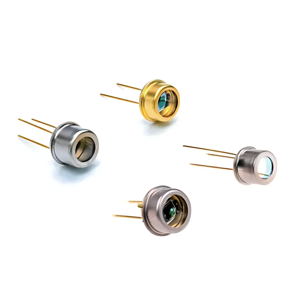
UV-Enhanced Silicon Photodiode
| Brand | Generic |
|---|---|
| Origin | Imported |
| Manufacturer Type | Distributor |
| Model | UV-Enhanced Silicon Photodiode |
| Pricing | Upon Request |
Overview
The UV-Enhanced Silicon Photodiode is a precision optoelectronic sensor engineered for high-sensitivity detection in the ultraviolet (UV) and near-visible spectral regions. Unlike standard silicon photodiodes—whose quantum efficiency drops sharply below 400 nm—this device features a specially optimized anti-reflection coating and surface passivation process that significantly extends spectral responsivity into the deep UV range (down to ~200 nm). It operates on the principle of the internal photoelectric effect: incident photons with energy exceeding the silicon bandgap (1.12 eV) generate electron-hole pairs in the depletion region, producing a photocurrent linearly proportional to irradiance under reverse or zero-bias conditions. Designed for integration into calibrated radiometric systems, UV-curing monitoring setups, ozone layer measurement instrumentation, and semiconductor lithography alignment tools, this photodiode delivers stable, low-noise performance in laboratory, industrial, and field-deployable optical test platforms.
Key Features
- Extended UV spectral response: Enhanced quantum efficiency from 200 nm to 1100 nm, with peak responsivity centered at λp ≈ 365 nm — ideal for mercury lamp lines and UV LED characterization.
- Low dark current: Typically < 50 pA at VR = 10 mV, enabling high signal-to-noise ratio (SNR) operation in low-light UV applications.
- Temperature-stable dark current behavior: Dark current temperature coefficient (Tcid) ≤ 1.05×/°C — critical for uncooled, long-duration measurements requiring minimal thermal drift correction.
- Low junction capacitance: Cj ≤ 15 pF at 0 V bias and 100 kHz, supporting fast transient response and compatibility with high-bandwidth transimpedance amplifiers.
- Rapid temporal response: Rise time tr ≤ 100 ns under zero-bias conditions — suitable for pulsed UV source characterization and time-resolved photometry.
- Hermetically sealed TO-can or surface-mount package options available — ensuring long-term stability in controlled-environment metrology labs and cleanroom-compatible manufacturing equipment.
Sample Compatibility & Compliance
This photodiode is compatible with standard UV-grade optical components including fused silica windows, MgF2 lenses, and broadband UV mirrors. Its active area geometry (typically 1 mm² to 5 mm²) supports both free-space beam coupling and fiber-optic interfacing via SMA905 or FC/PC adapters. The device conforms to JEDEC JESD22-A114 (ESD sensitivity Class 1B) and meets RoHS Directive 2011/65/EU requirements. While not certified to IEC 61000-4-x immunity standards as a standalone component, it is routinely integrated into systems compliant with ISO/IEC 17025-accredited calibration protocols for UV radiometry. Traceable NIST-calibrated responsivity data (A/W) is available upon request for each production lot, supporting GLP-compliant documentation workflows.
Software & Data Management
As a passive analog sensor, the UV-enhanced silicon photodiode does not incorporate embedded firmware or digital interfaces. However, it is fully interoperable with industry-standard data acquisition platforms—including National Instruments PXIe chassis with NI-9264 analog input modules, Keysight DAQ970A, and Thorlabs PM100D power meters—when paired with appropriate transimpedance gain stages and UV-calibrated reference sources. Raw photocurrent output is compatible with MATLAB, Python (via PyVISA or nidaqmx), and LabVIEW-based custom measurement suites. For traceable radiometric reporting, users may import factory-provided spectral responsivity curves (S(λ)) into software such as OceanView or LightMachinery’s SpectraSuite to perform wavelength-corrected irradiance calculations per ASTM E308-22 and CIE S 026/E:2019 guidelines.
Applications
- UV radiometric calibration of broadband and narrowband light sources (e.g., deuterium lamps, excimer lasers, UV-LED arrays)
- In-line monitoring of UV curing processes in adhesive, ink, and coating applications
- Ozone concentration sensing via 254 nm absorption spectroscopy
- Photolithography tool alignment and dose control in semiconductor fabrication facilities
- Environmental UV index instrumentation and solar UV-B monitoring networks
- Research-grade fluorescence excitation source characterization in life science imaging systems
FAQ
Is this photodiode suitable for vacuum-ultraviolet (VUV) measurements below 200 nm?
No — its enhanced UV response begins at ~200 nm; VUV detection (< 200 nm) requires specialized sensors such as Cs-Te photocathodes or silicon carbide (SiC) diodes.
Can it be operated under reverse bias to improve speed or linearity?
Yes — while optimized for zero-bias operation to minimize dark current, it supports reverse bias up to –10 V; consult the datasheet for breakdown voltage and linearity specifications at elevated bias.
Does the device include NIST-traceable calibration documentation?
Calibration certificates with spectral responsivity data (A/W vs. λ) are available as an optional add-on service per IEC 60794-1-21 Annex A compliance.
What mounting options are supported for OEM integration?
Standard configurations include TO-5, TO-8, and SMD packages (e.g., 3535 ceramic substrate); custom mechanical interfaces and hermetic window materials can be arranged through qualified distributors.
How does temperature affect responsivity stability over extended measurements?
Responsivity exhibits a typical temperature coefficient of –0.05 %/°C near λp; for metrology-grade applications, active temperature stabilization or post-acquisition thermal compensation algorithms are recommended.


 for EMI Conducted Emission & Immunity Testing")