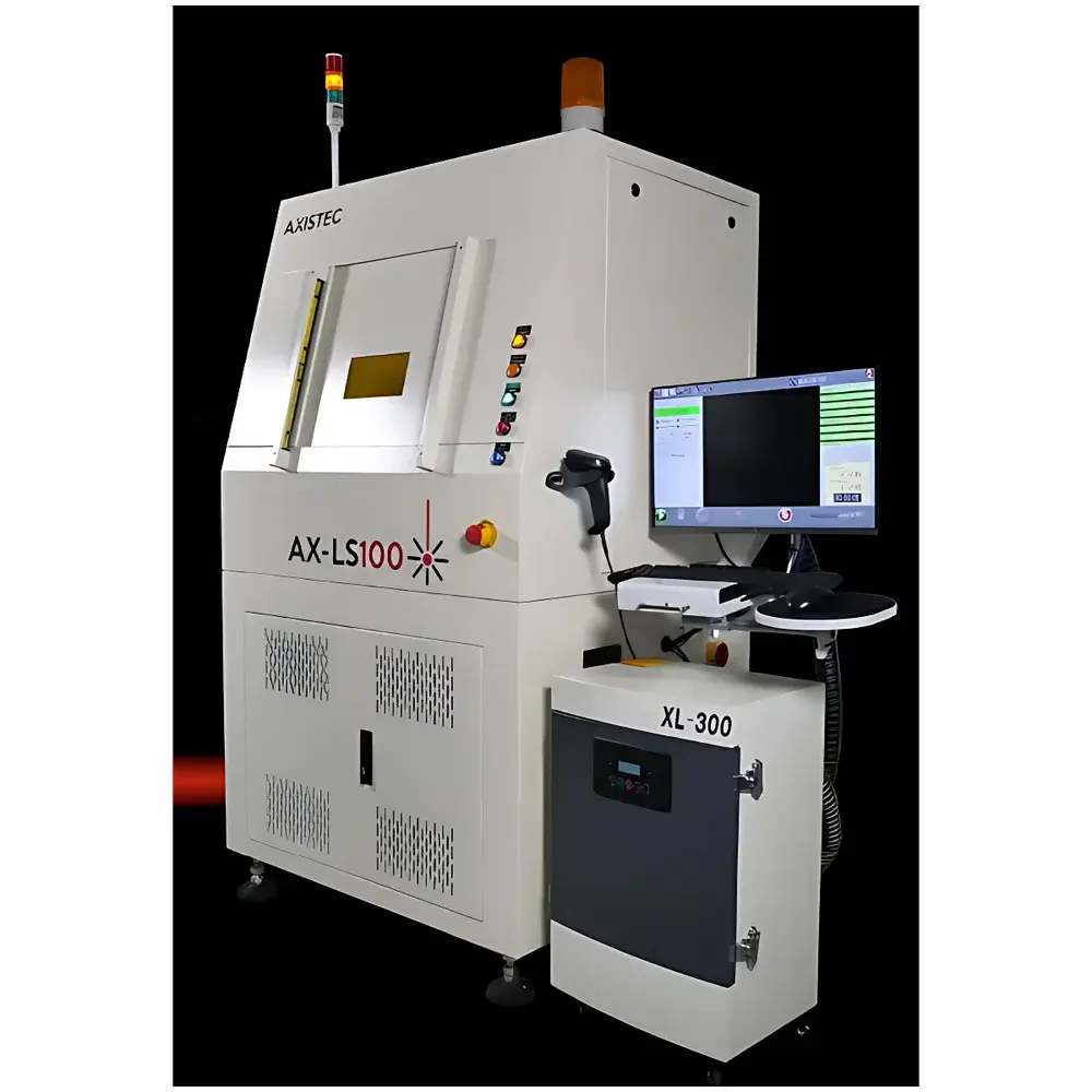
AXIS-TEC AX-LS1000 High-Precision Laser Dicing Saw
| Brand | AXIS-TEC |
|---|---|
| Origin | Singapore |
| Manufacturer Type | Authorized Distributor |
| Import Status | Imported |
| Model | AX-LS1000 |
| Maximum Linear Cutting Speed | 200 mm/s |
| Maximum Dicing Speed (YAG variant) | 140 mm/s |
| Maximum Dicing Speed (Semiconductor Laser variant) | 220 mm/s |
| Kerf Width | 30 µm |
| Cooling | Integrated Air-Cooling System |
| Configuration | T-Stage Dual-Station Platform |
| Laser Source Type | Fiber Laser (Standard), Optional YAG or Diode-Pumped Semiconductor Laser |
Overview
The AXIS-TEC AX-LS1000 is a high-precision, industrial-grade laser dicing saw engineered for non-contact, high-fidelity separation of brittle semiconductor and photovoltaic wafers. Unlike mechanical dicing saws that rely on diamond blades and generate mechanical stress, chipping, and debris, the AX-LS1000 employs focused fiber laser ablation—operating in the near-infrared spectrum (typically 1064 nm)—to achieve localized thermal decomposition with minimal heat-affected zones (HAZ). This enables clean, narrow kerfs (~30 µm), smooth sidewalls, and sub-micron positional repeatability—critical for thin-wafer handling (<100 µm), low-damage solar cell segmentation, and high-yield IC die singulation. Designed specifically for front-end and back-end semiconductor packaging workflows, the system supports both full-cut and stealth dicing modes, accommodating silicon (c-Si, mc-Si, a-Si), SiC, GaAs, and glass substrates used in PV modules, MEMS, and power devices.
Key Features
- T-stage dual-station architecture enables continuous loading/unloading while processing—eliminating idle time and increasing throughput by up to 35% versus single-station systems.
- Fiber laser source delivers TEM00 beam profile with M² < 1.1, ensuring diffraction-limited focusability and consistent energy density across the entire scan field.
- Air-cooled design reduces infrastructure dependency—no external chillers, water lines, or compressed air required—making it suitable for cleanroom Class 1000–10,000 environments and compact fab footprints.
- Modular mechanical platform conforms to SEMI S2/S8 safety standards; all optical enclosures meet IEC 60825-1 Class 4 laser safety requirements with interlocked access doors and real-time beam shutter control.
- Zero-consumable operation: no diamond blades, no coolant fluids, no flash lamps (in fiber configuration), and no periodic alignment recalibration—supporting >7,200 hours of uninterrupted runtime between service interventions.
Sample Compatibility & Compliance
The AX-LS1000 processes wafers ranging from 100 mm to 300 mm diameter and thicknesses from 50 µm to 1,000 µm. It accommodates standard FOUPs, FOSBs, and manual cassette loading via ergonomic height-adjustable stage interfaces. Compatible substrate materials include monocrystalline and polycrystalline silicon, amorphous silicon ribbons, silicon carbide (SiC), gallium arsenide (GaAs), sapphire, and fused silica. The system complies with ISO 9001:2015 manufacturing protocols and supports integration into ISO/IEC 17025-accredited laboratories. Optional audit-ready firmware packages provide electronic logbooks, user-access controls, and 21 CFR Part 11-compliant data integrity features—including operator authentication, timestamped event logging, and immutable parameter history—for GMP-aligned production environments.
Software & Data Management
Control is executed via AXIS-TEC’s proprietary DICE-PRO™ software suite—a Windows-based application built on .NET Framework with deterministic real-time motion control kernel. The GUI provides live path preview with overlay on CCD camera feed, layer-based job sequencing, automatic fiducial recognition (with sub-pixel accuracy), and parametric recipe management (pulse width, frequency, scan velocity, defocus offset). All process parameters are exportable in CSV/Excel format; raw sensor logs (laser power, stage position, temperature drift) are stored in SQLite databases with configurable retention policies. Remote diagnostics and firmware updates are supported over TLS-secured Ethernet connections, enabling predictive maintenance alerts based on cumulative laser diode operating hours and thermal gradient trends.
Applications
- Solar manufacturing: Precision scribing and separation of crystalline and thin-film photovoltaic cells—enabling high-efficiency tandem cell architectures and minimized material waste in ribbon-to-cell conversion.
- Semiconductor packaging: Die singulation of wafer-level chip-scale packages (WLCSP), fan-out wafer-level packages (FOWLP), and silicon photonics interposers where mechanical stress must be avoided.
- MEMS and sensors: Cleaving of fragile piezoelectric, capacitive, and inertial sensing dies without microcrack propagation or delamination.
- R&D prototyping: Rapid iteration of novel substrate stacks (e.g., heterojunction Si/perovskite) requiring sub-50 µm alignment tolerance and repeatable edge quality assessment per ASTM F3010-15.
FAQ
What laser wavelengths are supported on the AX-LS1000 platform?
The standard configuration uses a 1064 nm fiber laser; optional configurations include 532 nm (frequency-doubled) for transparent substrate processing and 355 nm (UV) for ultra-low HAZ applications on polymers and ceramics.
Does the system support automated wafer mapping and alignment?
Yes—integrated high-resolution CCD vision system with motorized zoom lens enables automatic wafer centering, notch/flat detection, and pattern-matching alignment using user-defined fiducials or die edge recognition algorithms.
Can the AX-LS1000 perform stealth dicing (SD) for silicon wafers?
Yes—when equipped with a picosecond pulsed fiber laser option and dynamic focus control, the system achieves subsurface modification at controlled depths (10–50 µm below surface), enabling post-process mechanical breakage with zero front-side damage.
Is the software compliant with industry traceability standards?
DICE-PRO™ includes configurable electronic signatures, role-based access levels, and tamper-evident audit trails meeting FDA 21 CFR Part 11, EU Annex 11, and ISO 13485 requirements for regulated medical device manufacturing.
What maintenance intervals are recommended for long-term reliability?
Under normal operation (8 h/day, 5 days/week), scheduled maintenance is required only every 12 months—limited to optical path inspection, stage rail lubrication, and calibration verification using NIST-traceable reference artifacts.


