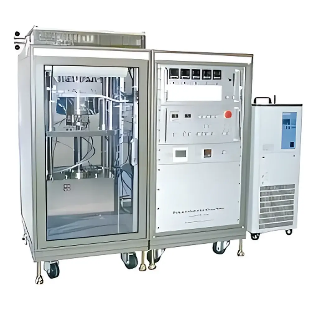
JAI SW-8400 & SW-12400 Single-Side Silicon Wafer Thermal Desorption Units for VOC Monitoring
| Brand | JAI |
|---|---|
| Origin | Japan |
| Model | SW-8400 (for 6"/8" wafers) & SW-12400 (for 12" wafers) |
| Instrument Type | Secondary Thermal Desorber |
| Desorption Temperature Range | Ambient to 500 °C |
| Desorption Recovery Rate | 70% |
| Sample Capacity | 1 wafer per run |
| Sealing Material | Polyimide O-ring (220 mm ID) |
| Cooling | Integrated water-circulation system |
| Safety Features | Overheat protection (15 A/30 mA), interlock mechanism, emergency stop button (red mushroom type), optional water-leak sensor |
| Power Supply | Single-phase AC 200 V, 15 A and AC 100 V, 20 A |
| Dimensions (W×H×D) | 1140 × 1106 × 750 mm |
| Weight | 280 kg |
Overview
The JAI SW-8400 and SW-12400 are dedicated single-side thermal desorption units engineered for quantitative volatile organic compound (VOC) monitoring on silicon wafers in semiconductor manufacturing and advanced materials R&D. Unlike conventional thermal desorbers designed for bulk sorbent tubes or environmental air sampling, these instruments implement an inverted furnace architecture that isolates and thermally desorbs VOCs exclusively from the front surface of a stationary silicon wafer—eliminating cross-contamination from backside outgassing or chamber wall contributions. The process follows ASTM D7339 and ISO 16000-6 principles for surface emission testing, adapted specifically for high-purity semiconductor substrates. Each unit integrates a transparent quartz heating furnace with independent top/bottom plate control, enabling precise thermal ramping and isothermal hold profiles up to 500 °C. The wafer is sealed against the furnace aperture using a high-temperature polyimide O-ring (220 mm inner diameter), ensuring leak-tight containment under inert purge gas (typically nitrogen, ≤500 mL/min). Desorbed analytes are swept directly into a primary adsorbent tube—commonly a 10 mL PAT tube packed with 2.5 g Tenax® GR—for subsequent transfer to GC or GC-MS. This configuration supports trace-level detection (sub-ng/cm² sensitivity) required for contamination control in 300 mm fab environments.
Key Features
- Inverted quartz furnace design ensures exclusive front-surface VOC capture—critical for process-critical wafer surface analysis.
- Independent dual-zone heating (top and bottom plates) enables uniform thermal distribution across 6″, 8″, or 12″ wafers, minimizing thermal gradient-induced analyte fractionation.
- Polyimide O-ring sealing (220 mm ID) provides hermetic closure at temperatures up to 500 °C without degradation or outgassing—validated per SEMI F57 standards for cleanroom-compatible materials.
- Integrated water-circulation cooling system maintains furnace structural integrity during repeated high-temperature cycles and enables rapid cooldown between runs.
- Comprehensive safety architecture includes current-based overheat detection (15 A trip, 30 mA sensing), mechanical interlock preventing furnace access during operation, red mushroom-type emergency stop, and optional water-leak sensor compliant with IEC 61508 functional safety requirements.
- Internally passivated insulation tubing and inert gas delivery lines minimize background interference—essential for low-part-per-quadrillion (ppq) detection limits in ultra-trace wafer surface analysis.
Sample Compatibility & Compliance
The SW-8400 accommodates 6″ and 8″ silicon wafers; the SW-12400 supports 12″ wafers—with optional extension rings available for sub-5″ substrates. Both models accept standard 1/16″–1/8″ gas fittings and interface directly with commercial thermal desorption–GC systems. Primary adsorbent tubes include proprietary PAT format (10 mL, 2.5 g Tenax GR), but universal adapters allow compatibility with alternative sorbent tubes (e.g., Carbopack™, Tenax-TA, or multi-bed configurations). All wetted surfaces undergo inertization via silanized or electroless nickel plating, meeting SEMI C12 and ISO 14644-1 Class 1 cleanroom particulate requirements. The system operates within GLP-compliant workflows and supports audit-ready operation when integrated with chromatography data systems (CDS) that comply with FDA 21 CFR Part 11 electronic record controls.
Software & Data Management
While the SW-8400/SW-12400 operate as hardware-controlled standalone modules, they feature analog/digital I/O ports (RS-232, 0–10 V analog output) for synchronization with external CDS platforms such as Thermo Chromeleon, Agilent OpenLab, or Waters Empower. Temperature ramp profiles, hold times, purge flow rates, and safety event logs are programmable via front-panel keypad or remote command set. All operational parameters—including real-time furnace temperature, coolant flow status, and interlock state—are timestamped and exportable in CSV format. When paired with validated CDS environments, full traceability is maintained per ISO/IEC 17025 and ASTM E2500-22 guidelines for analytical instrument qualification.
Applications
- Residual solvent and photoresist outgassing profiling on prime and test wafers pre- and post-lithography.
- Identification and quantification of airborne molecular contamination (AMC) sources in FOUPs, load ports, and track systems.
- Validation of wafer cleaning efficacy (e.g., SC-1, RCA, ozone treatments) via VOC removal kinetics.
- Failure analysis of gate oxide defects linked to volatile carbonaceous residues.
- Process window qualification for epitaxial growth and ALD precursors where surface adsorbate stability impacts nucleation uniformity.
FAQ
What wafer sizes does the SW-8400 support?
The SW-8400 is configured for 6-inch and 8-inch silicon wafers. Sub-5-inch wafers require an optional expansion ring.
Is the SW-12400 compatible with standard 12-inch FOUPs?
Yes—the SW-12400’s footprint and loading height are engineered to integrate with Class 1 automated material handling systems used in 300 mm fabs.
Can the system be validated for GMP environments?
Yes—when operated with documented IQ/OQ protocols and connected to a Part 11–compliant CDS, it meets core requirements for equipment qualification in regulated semiconductor process development labs.
What is the typical desorption recovery rate for chlorinated solvents?
Recovery rates vary by compound volatility and polarity; for common solvents like acetone, IPA, and NMP, average recoveries range from 65–75% under optimized 400 °C isothermal desorption with 5-minute hold.
Does the system include method development support?
JAI provides application notes aligned with SEMI standards and collaborates with certified third-party labs for method transfer and ruggedness testing per ICH Q2(R2).


")