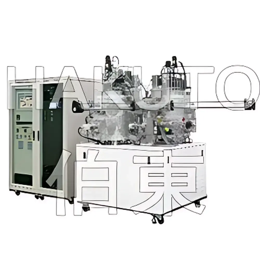
Syskey UHV Sputter System – High-Performance Magnetron Sputtering Deposition Tool for Semiconductor and Advanced Materials Research
| Brand | Syskey |
|---|---|
| Origin | Taiwan |
| Model | UHV Sputter |
| Baseplate Size | Up to 12-inch (300 mm) wafers |
| Substrate Temperature Range | Ambient to 1000 °C |
| Film Thickness Uniformity | ±3% |
| Ultimate Vacuum | ≤5×10⁻¹⁰ Torr |
| Sputter Sources | Up to 8 configurable magnetron cathodes (RF/DC/pulsed DC) |
| Gas Lines | Up to 4 mass flow-controlled channels (Ar, N₂, O₂, etc.) |
| Chamber Sealing | All-metal ConFlat (CF) flanges, bakeable to 150 °C |
| Substrate Manipulation | Motorized rotation with ceramic bearing & internal water cooling |
| Optional Integration | Load-lock, transfer chamber, glovebox, ion source (100 keV Kr⁺), e-beam evaporation, RGA/OES ports |
Overview
The Syskey UHV Sputter System is an engineered physical vapor deposition (PVD) platform designed for high-fidelity thin-film synthesis under ultra-high vacuum (UHV) conditions. Operating at ultimate pressures down to 5×10⁻¹⁰ Torr—achieved via all-metal CF-flanged construction, bakeable to 150 °C, and backed by cryogenic or turbo-molecular pumping—the system eliminates residual gas-phase contamination and minimizes surface reactivity during film growth. This UHV environment enables atomic-scale control over nucleation, interfacial chemistry, and stoichiometry in compound films such as NbTiN, SiO₂, Si₃N₄, Al₂O₃, Pd, and Nb. The system employs magnetron sputtering physics, where energetic argon ions bombard target surfaces in a confined magnetic field, enhancing plasma confinement and sputter yield while reducing substrate heating. Its architecture supports both sequential and co-sputtering configurations across up to eight independently controlled magnetron sources, making it suitable for multilayer heterostructures, graded compositions, and combinatorial materials screening in semiconductor process development and fundamental solid-state research.
Key Features
- UHV-compatible chamber with full ConFlat (CF) metal sealing and certified bakeability to 150 °C for outgassing control and long-term base pressure stability
- Motorized substrate rotation mechanism featuring high-purity ceramic bearings and integrated water-cooling to maintain mechanical integrity during extended 1000 °C thermal cycles
- Configurable magnetron array: up to eight RF/DC/pulsed-DC sputter sources with independent shuttering, adjustable target-to-substrate spacing, and optional 2–4 inch target compatibility
- Precision substrate heating: resistive heating capable of stable operation from ambient to 1000 °C with closed-loop thermocouple feedback and ±1 °C setpoint accuracy
- Multi-gas delivery: four independent MFC-controlled lines (Ar, N₂, O₂, reactive gases) with automated pressure regulation via Baratron capacitance manometer
- Integrated RF plasma cleaning (300 W, 13.56 MHz) for in-situ substrate surface preparation prior to deposition
- Expandable interface ports for RGA, OES, quartz crystal microbalance (QCM), and optional ion beam assistance (100 keV Kr⁺)
Sample Compatibility & Compliance
The Syskey UHV Sputter accommodates substrates up to 300 mm (12-inch) diameter, including silicon wafers, sapphire, fused silica, metallic foils, and flexible polymer templates. Substrate holders support flat, tilted, or rotating geometries, with custom fixturing available for non-planar or patterned samples. All wetted materials—including chamber walls, shields, and feedthroughs—are electropolished 316L stainless steel or oxygen-free copper to minimize metallic contamination and ensure compatibility with UHV-grade cleanliness protocols. The system complies with ISO 14644-1 Class 4 cleanroom integration standards and supports GLP/GMP-aligned operation through optional audit-trail-enabled software logging (21 CFR Part 11 compliant configuration available). It meets ASTM F2627–22 for sputter-deposited thin-film uniformity assessment and is routinely deployed in labs adhering to ISO/IEC 17025 accreditation requirements for materials characterization laboratories.
Software & Data Management
The system is operated via a Windows-based industrial HMI with deterministic real-time control of vacuum sequencing, gas flows, power delivery, temperature ramping, and shutter actuation. Process recipes—including multi-step sputter sequences, ramp/soak thermal profiles, and timed RF bias application—are stored with full version history and user-access permissions. All sensor data (pressure, temperature, power, flow rates, film thickness) are time-stamped and logged to SQL databases with configurable export (CSV, HDF5, MATLAB .mat). Optional integration with LabVIEW or Python APIs enables external automation, machine learning–driven parameter optimization, and synchronization with in-line metrology tools. Full audit trails—including operator ID, timestamp, parameter changes, and alarm events—are retained for regulatory review per FDA 21 CFR Part 11 and EU Annex 11 requirements.
Applications
This UHV sputtering platform serves mission-critical roles across multiple advanced technology domains. In semiconductor R&D, it fabricates gate dielectrics (Al₂O₃, HfO₂), diffusion barriers (TiN, TaN), and seed layers for Cu electroplating. In photovoltaics, it deposits transparent conductive oxides (ITO, AZO) and back-surface reflectors (Ag, Al) with sub-nanometer interfacial control. For quantum materials, it enables epitaxial growth of superconducting NbTiN films and topological insulator heterostructures requiring atomically clean interfaces. In MEMS/NEMS fabrication, it produces stress-engineered piezoresistive layers (SiCr, NiCr) and wear-resistant coatings (DLC, TiAlN). Academic and national lab users apply it to fundamental studies of interfacial diffusion kinetics, oxidation mechanisms under controlled partial pressures, and defect-mediated charge transport in oxide semiconductors.
FAQ
What vacuum level is required for reproducible stoichiometric oxide film growth?
For consistent metal–oxygen bonding in films like SiO₂ or Al₂O₃, base pressures ≤1×10⁻⁹ Torr and process pressures <5×10⁻³ Torr (with active O₂ partial pressure control) are recommended to suppress hydrocarbon incorporation and ensure repeatable O/Metal ratios.
Can the system be configured for in-situ XRD or XPS analysis?
Yes—the chamber includes standard DN63CF and DN100CF viewports with anti-reflective fused silica or MgF₂ windows, plus dedicated UHV-transfer ports compatible with commercial load-lock–equipped surface science systems.
Is remote diagnostics and preventive maintenance supported?
All critical subsystems (pumps, gauges, power supplies, MFCs) report health status via Modbus TCP; predictive alerts for pump oil degradation, gauge calibration drift, and cathode arcing frequency are enabled through optional cloud-connected firmware.
How is film thickness monitored during deposition?
Standard integration includes a dual-channel quartz crystal microbalance (QCM) with ±0.1 Å resolution; optional laser interferometry or ellipsometry ports support real-time optical thickness tracking for transparent or absorbing layers.
What safety certifications does the system meet?
The platform conforms to CE marking (EMC Directive 2014/30/EU, Machinery Directive 2006/42/EC), UL 61010-1 for electrical safety, and ISO 12100 risk assessment methodology—with interlocked access doors, emergency stop circuits, and redundant vacuum venting logic.


