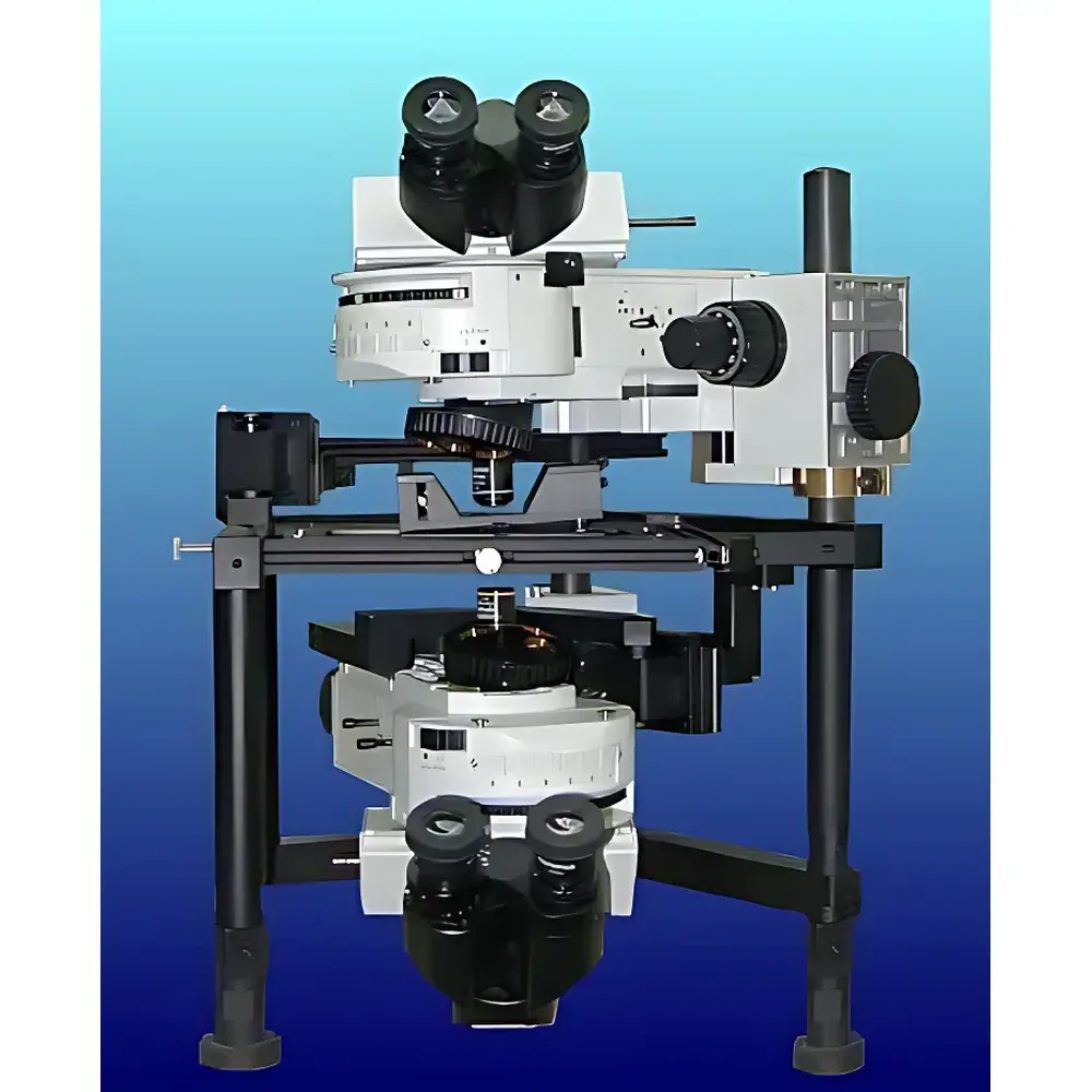
Nanonics MultiView2000 Atomic Force Microscope
| Brand | Nanonics |
|---|---|
| Origin | Israel |
| Model | MultiView2000 |
| Instrument Type | Materials-Focused AFM/NSOM Hybrid System |
| Scan Mode | Tip Scanning |
| XY Resolution | <5 nm |
| Z Resolution | <1 nm |
| XY Scan Range | 70 µm (standard), optional 30 µm and 10 µm scanners |
| Z Scan Range | 70–120 µm |
| XY Step Size | <1 nm (70 µm scanner), <0.1 nm (10 µm scanner) |
| Scanner Thickness | 7 mm |
| Scanner Mass | 75 g |
| Max Sample Radius | 16 mm (customizable) |
| Probe Compatibility | Full commercial SPM probe interoperability including NSOM, conductive AFM, hollow probes, insulated nanowire sensors, dual-wire glass-insulated probes, low-k modulus probes, and deep-trench AFM probes |
| Operational Modes | NSOM reflection/transmission/collection/near-field fluorescence/PL |
| Controller | Nanonics Analog Controller with NT software (Windows 95/98/XP compatible) |
| Environmental Capabilities | Cryogenic operation down to 4 K (liquid helium), UHV compatibility, integrated gas/liquid delivery, in situ reaction chamber, co-located optical microscopy and micro-Raman coupling |
Overview
The Nanonics MultiView2000 is a high-precision, multi-modal scanning probe microscope engineered for simultaneous and correlative atomic force microscopy (AFM) and near-field scanning optical microscopy (NSOM). Developed by Nanonics Imaging Ltd.—a pioneer in hybrid near-field instrumentation since 1997—the system integrates piezoelectric tip-scanning architecture with modular optical pathways to enable quantitative nanoscale topographic, mechanical, optical, thermal, and electrical characterization. Its core measurement principle relies on dynamic or static force feedback between a sharp probe and sample surface (AFM), combined with sub-diffraction-limit optical excitation and collection via tapered, metal-coated optical fibers (NSOM). This dual-mode capability allows users to acquire co-registered topography, nanomechanical properties (e.g., elasticity, adhesion, dissipation), and localized optical responses (fluorescence, photoluminescence, Raman enhancement) within the same scan area—without repositioning or compromising spatial registration. Designed for materials science laboratories requiring rigorous metrology under controlled environments, the MultiView2000 supports operation from ambient air through inert gas, liquid immersion, ultra-high vacuum (UHV), and cryogenic conditions down to 4 K.
Key Features
- Modular tip-scanning architecture with interchangeable scanners: standard 70 µm XY range (sub-nm step resolution), plus optional 30 µm and high-resolution 10 µm scanners (<0.1 nm step size)
- Integrated Nanonics Analog Controller with NT software suite—enabling real-time 8-channel image acquisition, 3D surface reconstruction, spectral overlay, and batch analysis
- Full commercial probe interoperability: compatible with all major SPM probe types—including NSOM fiber probes, conductive and non-conductive AFM cantilevers, low-stiffness polymer probes, deep-trench silicon probes, hollow-fluidic probes, and glass-insulated nanowire sensors
- Dual-path optical integration: supports simultaneous far-field confocal imaging (transmission/reflection/fluorescence) and near-field optical signal collection across UV–VIS–NIR spectra
- Environmental flexibility: built-in reaction chamber with automated gas/liquid delivery, temperature control stages (cryo- and heating), and UHV-ready mechanical design
- Multi-instrument synchronization interface: native support for real-time correlation with SEM, micro-Raman spectrometers, SHG systems, and thermal analysis modules
Sample Compatibility & Compliance
The MultiView2000 accommodates samples up to 16 mm radius (customizable per application), including conductive, insulating, soft biological, and heterogeneous thin-film substrates. Its open-probe architecture permits in situ functionalization, electrochemical biasing, and localized fluidic injection during scanning. The system meets key international standards for nanometrology traceability, including ISO/IEC 17025-compliant calibration protocols for lateral and vertical resolution verification. For regulated environments, the NT software platform supports audit-trail logging and user-access controls aligned with FDA 21 CFR Part 11 requirements when deployed in GMP/GLP-compliant labs. All mechanical and electronic subsystems conform to CE and RoHS directives; vacuum and cryogenic modules comply with ISO 27465 (vacuum integrity) and ASTM E2584 (low-temperature instrumentation safety).
Software & Data Management
The proprietary NT software provides a unified interface for instrument control, multi-channel data acquisition, and advanced post-processing. It supports real-time overlay of topographic, phase, amplitude, current, and optical intensity maps—each stored with full metadata (scan parameters, environmental conditions, probe ID, calibration history). Raw data is saved in vendor-neutral HDF5 format, enabling direct import into MATLAB, Python (via h5py), or third-party analysis suites such as Gwyddion and SPIP. The LabVIEW-compatible DAQ module enables custom automation workflows, including closed-loop feedback control for force spectroscopy or optothermal triggering. All software modules undergo annual validation against NIST-traceable reference standards; version-controlled updates are delivered with documented change logs and impact assessments for regulated users.
Applications
- Materials Science: Quantitative nanomechanical mapping of polymer blends, graphene domain boundaries, and battery electrode interfaces; roughness, adhesion hysteresis, and viscoelastic relaxation analysis under variable humidity or temperature
- Life Sciences: Live-cell membrane dynamics in physiological buffer; nanoscale pore distribution in lipid bilayers; correlative AFM-NSOM imaging of labeled intracellular structures without fixation artifacts
- Semiconductor Metrology: Sub-10 nm gate oxide thickness profiling; dopant concentration gradients via Kelvin probe force microscopy (KPFM) integration; defect localization in EUV photoresists
- Data Storage: Magnetic domain contrast in perpendicular recording media; head-disk interface wear simulation; nanoscale friction anisotropy mapping on textured lubricated surfaces
- Nanophotonics: Plasmonic hotspot localization on metamaterial arrays; exciton diffusion length measurement in 2D semiconductors using time-resolved NSOM-PL; waveguide mode profiling in integrated photonic circuits
- Fundamental Physics: Quantum dot emission mapping at cryogenic temperatures; vortex lattice imaging in type-II superconductors; strain-induced bandgap modulation in heterostructured TMDs
FAQ
Does the MultiView2000 support true simultaneous AFM and NSOM acquisition?
Yes—the system employs synchronized dual-loop control where topographic feedback (AFM) and optical signal detection (NSOM) operate in parallel with sub-pixel spatial registration maintained via hardware-level trigger alignment.
Can I use third-party SPM probes without modification?
Absolutely—all commercially available probes—including those from Bruker, NanoAndMore, and Olympus—are mechanically and electrically compatible without adapters or firmware patches.
Is cryogenic NSOM operation validated below 10 K?
Yes—integrated liquid helium cryostat configurations have been independently verified to maintain <1 nm Z stability and <5 nm XY resolution at 4.2 K, with published benchmark data available upon request.
How is data integrity ensured during long-duration scans in regulated environments?
NT software enforces automatic checksum generation, timestamped operator authentication, and immutable audit trails compliant with 21 CFR Part 11 Annex 11 requirements for electronic records and signatures.
What optical coupling options are available for micro-Raman integration?
The system includes standardized kinematic mounts and fiber-coupled ports compatible with Horiba, WITec, and Renishaw Raman platforms, enabling simultaneous tip-enhanced Raman scattering (TERS) and AFM-NSOM acquisition.


