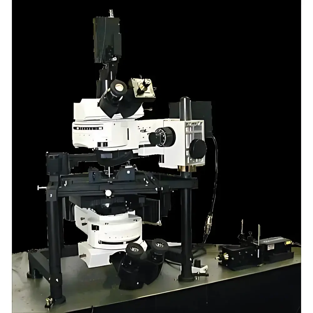
Nanonics MultiView4000 Atomic Force Microscope
| Brand | Nanonics |
|---|---|
| Origin | Israel |
| Model | MultiView4000 |
| Instrument Type | Material-Focused AFM |
| Positioning Noise | XY < 20 nm |
| Sample Dimensions | Ø < 100 mm |
| Stage Travel Range | 170 µm × 170 µm |
| XY Resolution | < 5 nm |
| Z Resolution | < 1 nm |
| Scan Range (Combined Piezo + Sample Scanner) | up to 160 µm (XY) |
| Minimum Step Size | < 0.1 nm (10 µm scanner) |
| Scanner Thickness | 7 mm |
| Mass | 75 g |
| Probe Compatibility | Commercial SPM, NSOM, conductive, hollow, insulated glass nanowire, dual-wire, low-k AFM, deep-trench AFM probes |
| Operating Modes | NSOM reflection/transmission/collection/fluorescence/PL |
Overview
The Nanonics MultiView4000 Atomic Force Microscope is a high-precision, multi-modal scanning probe platform engineered for integrated nanoscale characterization across materials science, semiconductor metrology, life sciences, and quantum device research. Unlike conventional standalone AFMs, the MultiView4000 implements a true hybrid architecture—co-locating atomic force sensing with near-field optical microscopy (NSOM), micro-Raman spectroscopy, SEM, confocal fluorescence, ion beam, and thermal analysis modules on a single, mechanically stable stage. Its core measurement principle relies on piezoelectrically driven tip-sample interaction in contact, tapping, or non-contact AFM modes, coupled with sub-diffraction-limit optical excitation and collection via aperture-based or apertureless NSOM probes. This enables simultaneous topographic, mechanical (elastic modulus, adhesion, dissipation), electrical (C-AFM, KPFM), thermal (SThM), and optical (fluorescence lifetime, PL mapping, Raman shift) data acquisition—all spatially registered at <5 nm lateral and <1 nm vertical resolution.
Key Features
- Modular integration-ready design supporting concurrent or sequential operation of AFM, NSOM, micro-Raman, SEM, and confocal optical modules without realignment.
- Dual-scanner architecture: high-resolution 10 µm scanner (<0.1 nm step size) nested within a 170 µm travel sample stage—enabling large-area navigation followed by nanometer-precision local interrogation.
- Low-noise positioning system with XY < 20 nm and Z < 0.3 nm thermal/mechanical drift over 1 hour—critical for long-duration spectroscopic mapping and time-lapse biological imaging.
- Universal probe compatibility: accepts commercial SPM cantilevers, metal-coated NSOM fibers, insulated glass nanowires, hollow-fluidic probes, and custom-fabricated low-stiffness (<0.01 N/m) or high-aspect-ratio trench probes.
- Environmental flexibility: fully compatible with cryogenic stages (down to 4 K), ultra-high vacuum (UHV) chambers (<10⁻¹⁰ mbar), controlled gas/liquid flow cells, and electrochemical cells for in situ and operando studies.
- Compact scanner geometry: 7 mm thickness and 75 g mass minimize inertial coupling and acoustic sensitivity—ideal for vibration-isolated optical tables and cleanroom integration.
Sample Compatibility & Compliance
The MultiView4000 accommodates samples up to 100 mm in diameter and 15 mm in thickness, with optional custom stage configurations available for wafer-scale (200 mm/300 mm) or irregular substrates. Its open-access design permits direct integration with third-party optical microscopes, laser sources (CW/pulsed, UV–IR), and detector systems (EMCCD, APD, spectrometers). From a regulatory standpoint, the system supports GLP/GMP-compliant workflows through audit-trail-enabled software logging (per FDA 21 CFR Part 11 requirements), standardized metadata embedding (according to ISO/IEC 17025 and ASTM E2500), and traceable calibration protocols for height, force, and optical intensity channels.
Software & Data Management
Control and analysis are executed via Nanonics’ NT software suite (Windows-compatible), offering real-time 8-channel image acquisition, cross-correlative overlay (e.g., AFM topography + NSOM fluorescence + Raman spectral map), and batch-processing pipelines for roughness, grain statistics, force-distance curve fitting, and autocorrelation analysis. LabVIEW-based APIs enable full hardware-level scripting for custom feedback loops, synchronized stimulus-response experiments (e.g., voltage-triggered PL quenching), and integration into automated fabrication lines. All raw data adhere to HDF5 format with embedded instrument parameters, environmental logs, and user annotations—ensuring FAIR (Findable, Accessible, Interoperable, Reusable) compliance for institutional repositories and collaborative projects.
Applications
- Materials Science: Quantitative nanomechanical mapping of polymer blends, 2D materials (graphene, TMDCs), and MOFs—including elastic modulus, loss tangent, and viscoelastic relaxation under controlled humidity or temperature.
- Semiconductor Metrology: High-resolution trench depth profiling, sidewall angle measurement, dopant distribution via Kelvin probe force microscopy (KPFM), and gate oxide defect localization.
- Life Sciences: Live-cell membrane dynamics in physiological buffer, virus–host receptor binding kinetics, and subcellular organelle stiffness gradients—enabled by low-force liquid-phase AFM and NSOM fluorescence co-imaging.
- Photonics & Plasmonics: Near-field optical mapping of localized surface plasmon resonances (LSPRs), photonic crystal bandgap verification, and exciton diffusion length quantification in perovskite thin films.
- Failure Analysis: Correlative topographic–electrical–optical inspection of interconnect voids, solder joint fatigue, and dielectric breakdown sites in advanced packaging.
FAQ
Is the MultiView4000 compatible with third-party SPM controllers or software?
Yes—the system provides TTL, analog, and USB interfaces for external synchronization, and its NT software supports import/export of standard SPM file formats (Gwyddion, WSxM, SPIP) and Python/Matlab APIs.
Can NSOM and AFM measurements be performed simultaneously on the same region?
Yes—dual-probe configurations (e.g., AFM tip + NSOM fiber) allow concurrent topographic and near-field optical data acquisition with pixel-by-pixel spatial registration.
What level of vacuum or cryogenic performance is certified?
The base platform is UHV-ready (with optional bake-out ports and all-metal seals); cryogenic operation down to 4 K has been validated using commercially available closed-cycle refrigerators and exchange-gas cryostats.
Does the system support quantitative force spectroscopy?
Yes—force-distance curves are acquired with calibrated photodiode detection, thermal tune-based spring constant calibration, and drift-compensated approach-retract cycles meeting ISO 11393-1 standards.
Are application-specific probe sets available from Nanonics?
Yes—Nanonics offers pre-characterized probe kits for biological NSOM, low-k dielectric metrology, high-aspect-ratio trench imaging, and combined conductive/thermal AFM, each supplied with individual calibration certificates.


