Mikropack SpecEL-2000-VIS Spectroscopic Ellipsometer
| Origin | Germany |
|---|---|
| Manufacturer Type | Authorized Distributor |
| Origin Category | Imported Instrument |
| Model | SpecEL-2000-VIS |
| Pricing | Upon Request |
Overview
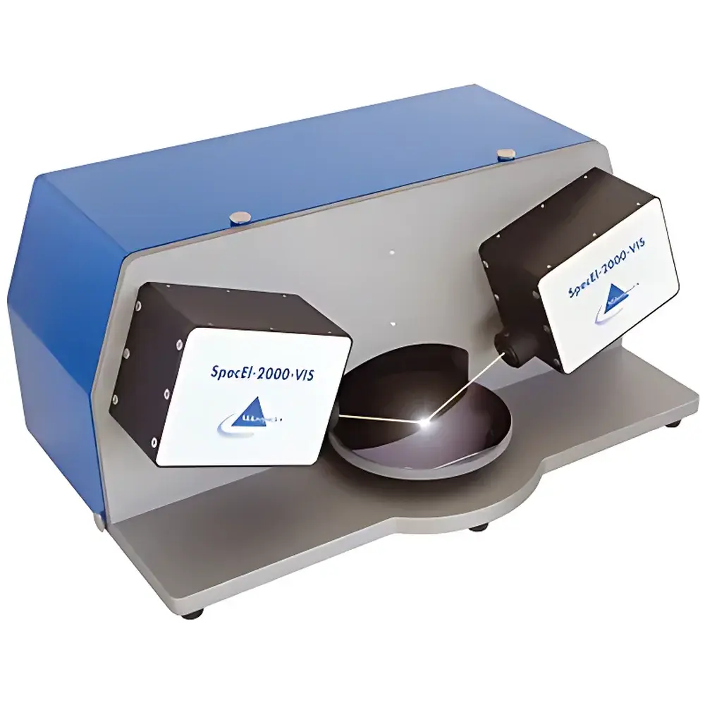
The Mikropack SpecEL-2000-VIS is a compact, benchtop spectroscopic ellipsometer engineered for high-precision, non-destructive characterization of thin films and surface layers. Based on the fundamental principles of ellipsometry—measuring the change in polarization state (amplitude ratio Ψ and phase difference Δ) of light upon reflection from a sample—the instrument delivers quantitative optical constants (refractive index n and extinction coefficient k) and film thickness across the visible spectral range (450–900 nm). Unlike intensity-based reflectometry, ellipsometry is inherently insensitive to light source fluctuations and ambient stray light, enabling superior reproducibility and stability in routine QC and R&D environments. The system operates at a fixed angle of incidence of 70°, optimized for high sensitivity to sub-nanometer thickness variations and dielectric property gradients in transparent or semi-transparent substrates such as silicon wafers, fused silica, BK7 glass, and ITO-coated surfaces.
Key Features
- Integrated broadband illumination: Built-in stabilized halogen-tungsten light source with optimized spectral output across 450–900 nm
- Compact optomechanical architecture: Total footprint of 52 × 33 × 24 cm; designed for space-constrained cleanrooms and lab benches
- Fixed-angle configuration: Precisely aligned 70° incidence geometry ensures consistent measurement conditions and eliminates angular calibration drift
- High-speed acquisition: Full-spectrum Ψ(λ) and Δ(λ) data acquired in 5–15 seconds per measurement point
- Sub-nanometer resolution: Capable of resolving film thicknesses from 0.1 nm to 8 µm with ±1 nm repeatability under controlled environmental conditions
- Modular optical path: Includes polarizer, sample stage with manual XYZ adjustment, analyzer, and enhanced collection optics coupled to a miniature linear CCD spectrometer
- Optional micro-spot module: Reduces incident beam size from standard 2 × 4 mm to 200 × 400 µm for localized analysis of patterned wafers or heterogeneous samples
Sample Compatibility & Compliance
The SpecEL-2000-VIS accommodates flat, rigid substrates up to 150 mm in diameter, including polished silicon, quartz, sapphire, and coated glass. It supports single-layer and multilayer stack analysis (e.g., SiO₂/SiNₓ on Si, polymer-on-glass, metal-dielectric stacks), provided interfacial roughness remains below 1 nm RMS and layer uniformity meets standard ellipsometric modeling assumptions. The system complies with ISO/IEC 17025 requirements for measurement traceability when operated with certified reference standards. Data acquisition and reporting workflows align with GLP and GMP documentation practices, supporting audit-ready export of raw spectra, fitted models, and parameter uncertainty estimates.
Software & Data Management
The included 32-bit Windows-based control and analysis software provides full instrument automation, real-time spectral visualization, and advanced regression fitting using physically grounded dispersion models—including Cauchy, OJL, Tauc-Lorentz, Drude, EMA, and multi-oscillator formulations. Users can define custom layer structures, assign material libraries, and apply constraints based on prior knowledge (e.g., fixed bandgap, known stoichiometry). The software stores validated measurement protocols—including substrate selection, model initialization, and convergence criteria—as reusable templates, minimizing operator-dependent variability. All raw and processed data are saved in open ASCII formats (.txt, .csv) and HDF5-compliant binary files, facilitating integration with LIMS platforms and third-party analysis tools. Audit trail functionality logs user actions, timestamped parameter changes, and fit residuals—supporting compliance with FDA 21 CFR Part 11 where electronic signatures and record integrity are required.
Applications
- Process development and monitoring of PVD, CVD, ALD, and spin-coated thin films in semiconductor and photovoltaic fabrication
- Optical coating verification (anti-reflective, high-reflection, filter stacks) in precision optics manufacturing
- Characterization of transparent conductive oxides (TCOs), perovskite absorber layers, and organic semiconductors in R&D labs
- Quality control of protective coatings on medical devices and display substrates
- Academic research in surface science, nanomaterials, and soft matter interfaces
FAQ
What is the minimum measurable film thickness?
The system achieves reliable thickness quantification down to 0.1 nm for high-contrast dielectric films on reflective substrates (e.g., SiO₂ on Si), subject to surface cleanliness and measurement repeatability.
Can the SpecEL-2000-VIS measure rough or textured surfaces?
It is optimized for smooth, planar samples. For moderately rough surfaces (RMS < 2 nm), effective medium approximation (EMA) modeling may be applied—but accuracy degrades with increasing topography beyond this threshold.
Is the software compatible with modern Windows operating systems?
The native application runs on Windows 7 through Windows 11 (32-bit compatibility mode enabled); full 64-bit support is available via Mikropack’s current-generation software suite (optional upgrade).
Does the system require external calibration standards?
No routine recalibration is needed. Factory alignment and wavelength calibration are stable over time; optional NIST-traceable Si wafer standards are available for periodic verification.
Can the instrument be integrated into automated production lines?
Yes—via RS-232 and TCP/IP interfaces, the SpecEL-2000-VIS supports remote command execution and data streaming for inline process monitoring when paired with appropriate motion stages and environmental enclosures.


