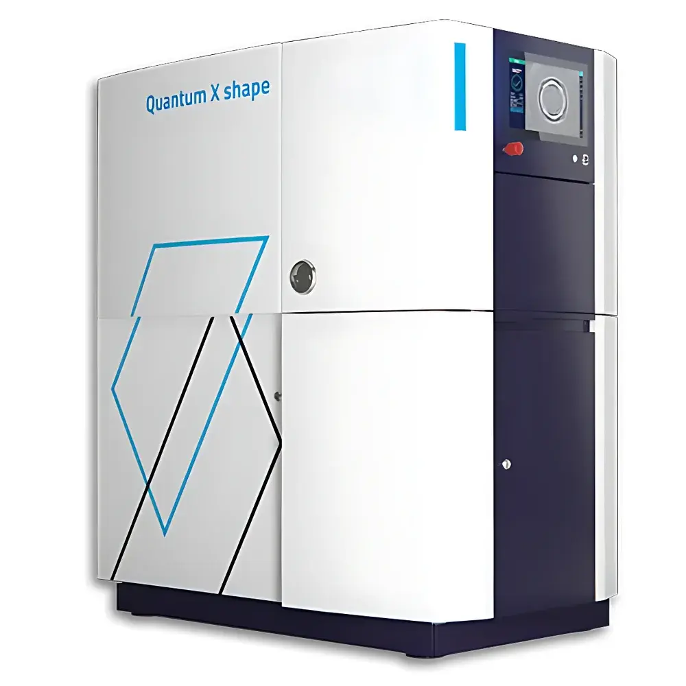
Nanoscribe Quantum X shape Direct-Write Two-Photon Lithography System
| Brand | Nanoscribe |
|---|---|
| Origin | Germany |
| Manufacturer Type | Authorized Distributor |
| Origin Category | Imported |
| Model | Quantum X shape |
| Exposure Mode | Proximity-Based Two-Photon Absorption |
| Resolution | 100 nm (feature size) |
| Light Source | Femtosecond Pulsed Near-Infrared Laser |
| Wavelength | 780 nm |
| Intensity Uniformity | ±1% |
| Maximum Exposure Area | 100 mm diameter |
| Surface Roughness (Ra) | ≤ 5 nm |
| Shape Accuracy | ≤ 200 nm |
| Single Print Field Diameter | ≥ 4,000 µm |
| Max Scanning Speed | 6.25 m/s (at 10× objective) |
| Substrate Compatibility | Up to 200 mm (8″) wafers, glass, silicon, opaque substrates |
| Compatible Photoresists | Nanoscribe IP-series (polymer), GP-Silica (glass-like), and third-party resists |
Overview
The Nanoscribe Quantum X shape is a high-precision, industrial-grade direct-write two-photon lithography (TPL) system engineered for sub-100 nm 3D micro- and nanofabrication. Unlike conventional photolithography or mask-based approaches, it employs nonlinear optical excitation—specifically, femtosecond-pulsed two-photon absorption at 780 nm—to induce localized polymerization within photosensitive resists. This enables true volumetric, layerless fabrication with isotropic resolution down to 100 nm in all three spatial dimensions, independent of substrate topography. Designed for both research laboratories and pilot-scale production environments, the Quantum X shape integrates a granite-based mechanical platform with active vibration damping and thermal stabilization, ensuring long-term positional fidelity and repeatability across multi-hour print jobs. Its architecture supports wafer-level processing up to 200 mm (8-inch), making it uniquely suited for applications demanding metrological-grade accuracy, structural fidelity, and process scalability.
Key Features
- Sub-100 nm feature resolution enabled by adaptive voxel control and grayscale TPL, allowing precise modulation of local refractive index and material density.
- Large-field printing capability: ≥4,000 µm single-field diameter with seamless stitching across 50 × 50 mm² maximum build area.
- High-throughput operation: Up to 200 standardized mesoscale structures printed overnight under unattended conditions.
- Robust mechanical design featuring a monolithic granite base, air-damped optical table integration, and temperature-stabilized laser path alignment.
- Flexible substrate handling: Supports standard microscope slides (76 × 26 mm²), silicon wafers (25.4–200 mm), fused silica, and other optically opaque or reflective substrates.
- Multi-resist compatibility: Fully optimized for Nanoscribe IP-L and GP-Silica photoresists; validated interface for third-party and custom-developed resins including hybrid organic-inorganic formulations.
Sample Compatibility & Compliance
The Quantum X shape accommodates diverse substrate materials—including silicon, glass, sapphire, metals (with appropriate adhesion layers), and flexible polymers—without requiring conductive coatings or vacuum environments. All hardware and software modules comply with CE marking requirements and meet electromagnetic compatibility (EMC) standards per EN 61326-1. The system supports GLP-compliant documentation workflows, including audit-trail-enabled job logging, user-access controls, and timestamped parameter archiving—facilitating traceability in regulated development settings. While not certified for ISO 13485 or FDA 21 CFR Part 11 out-of-the-box, its data management architecture is fully compatible with enterprise-grade LIMS and QMS platforms used in medical device prototyping and semiconductor R&D.
Software & Data Management
Nanoscribe’s proprietary Quantum X software provides an integrated environment for CAD-to-print workflow execution—from STL/OBJ import and lattice structure generation to path planning, exposure dose calibration, and real-time scan monitoring. The software includes built-in compensation algorithms for optical aberrations, stage drift correction, and resist-specific development shrinkage modeling. Export formats include G-code (for external post-processing), HDF5 (for scientific analysis), and standardized TIFF stacks for SEM/AFM correlation. All print parameters, metadata, and raw scan logs are stored in encrypted SQLite databases with configurable backup intervals and network share synchronization—ensuring full reproducibility and compliance with institutional data governance policies.
Applications
- Life Sciences: Fabrication of biomimetic scaffolds, microfluidic organ-on-chip devices, and high-aspect-ratio neural electrode interfaces with subcellular feature fidelity.
- Materials Engineering: Design and realization of metamaterials, programmable auxetics, and hierarchical porous architectures for catalysis and filtration.
- Microfluidics: Monolithic integration of valves, mixers, and droplet generators directly into PDMS-compatible master molds or glass chips.
- MEMS & Micro-Mechanics: Functional micro-springs, resonators, and flexure hinges with controlled stress distribution and fatigue-resistant geometry.
- Refractive & Diffractive Micro-Optics: Achromatic microlens arrays, freeform waveguides, and polarization-selective diffractive elements for AR/VR and LiDAR systems.
- Integrated Photonics: Low-loss 3D waveguide interconnects, photonic crystal cavities, and mode converters fabricated directly on SOI or SiN platforms.
FAQ
What is the minimum printable feature size, and how is it verified?
The system achieves a guaranteed minimum feature size of 100 nm in x-, y-, and z-directions, as validated using calibrated TEM grids and AFM line profiling on IP-L resist structures under standardized exposure and development protocols.
Can the Quantum X shape be integrated into a cleanroom environment?
Yes—it meets ISO Class 5 (Class 100) particulate limits when operated with optional HEPA-filtered enclosure kits and is compatible with standard semiconductor fab utility interfaces (dry N₂ purge, chilled water, grounded power).
Is wafer-level alignment supported for overlay lithography?
The system includes optional fiducial-based alignment routines enabling registration accuracy better than ±250 nm relative to pre-patterned marks—suitable for iterative multi-layer 3D structuring on processed wafers.
How does two-photon lithography differ from UV projection lithography in terms of resolution and depth control?
Unlike diffraction-limited UV projection, TPL relies on nonlinear absorption confined to the laser focus volume, enabling true 3D voxel placement without masks or proximity gaps—and eliminating sidewall taper or standing-wave effects inherent in planar processes.
What training and support options are available for new users?
Nanoscribe offers on-site installation commissioning, hands-on operator certification workshops, and remote application engineering support—with dedicated access to application notes, SOP templates, and quarterly technical webinars focused on advanced resist processing and metrology correlation.


