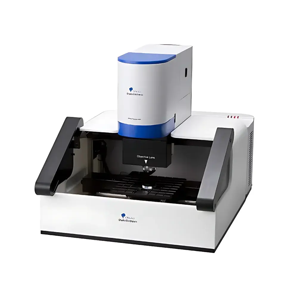
Otsuka OPTM Micro-Spectrophotometric Thin-Film Thickness Analyzer
| Brand | Otsuka Electronics |
|---|---|
| Origin | Japan |
| Model | OPTM |
| Measurement Principle | Spectral Interferometry |
| Optical Range | UV–NIR (e.g., 200–1100 nm) |
| Measurement Speed | <1 sec per point |
| Sample Stage | Motorized Auto XY Stage (standard) |
| Reflectance Accuracy | High-fidelity absolute reflectance measurement |
| Output Data | Film thickness (nm), refractive index (n), extinction coefficient (k) |
| Compliance | Designed for ISO/IEC 17025-aligned QC environments, supports GLP/GMP traceability workflows |
| Customization | Optional embedded probe head, fixed-stage configurations, user-defined measurement sequences |
Overview
The Otsuka OPTM Micro-Spectrophotometric Thin-Film Thickness Analyzer is an engineered solution for non-contact, high-precision optical characterization of thin films using spectral interferometry. Unlike conventional ellipsometers or single-wavelength reflectometers, the OPTM integrates a micro-optical spectrophotometric head with a high-resolution imaging system to acquire absolute reflectance spectra across a broad UV–NIR range (typically 200–1100 nm). This spectral signature serves as the primary input for rigorous inverse modeling—enabling simultaneous determination of film thickness (in nanometers), complex refractive index (n + ik), and multilayer stack architecture. The system operates on first-principles optical modeling, solving the Fresnel equations iteratively to match measured and simulated reflectance curves. Its design targets R&D laboratories developing optical coatings, semiconductor passivation layers, OLED encapsulation stacks, and photovoltaic absorber films—where sub-nanometer thickness resolution and quantitative n/k extraction are critical for process control and material validation.
Key Features
- Integrated micro-spectrophotometric head with high-throughput optics optimized for absolute reflectance acquisition—not relative or normalized values—ensuring metrological traceability.
- Sub-second single-point measurement cycle (<1 s), enabled by a high-sensitivity area sensor and optimized spectral calibration protocol.
- UV–NIR broadband detection (200–1100 nm) supports characterization of wide-bandgap dielectrics (e.g., SiO₂, Al₂O₃), transparent conductive oxides (ITO), and absorbing layers (e.g., a-Si, perovskites).
- Motorized XYZ stage with optional auto-focus and pattern-recognition alignment—standard configuration includes precision XY translation for wafer-scale mapping.
- Modular hardware architecture permitting embedded probe integration for in-line or tool-integrated deployment (e.g., cluster tools, vacuum chambers, roll-to-roll lines).
- User-configurable measurement sequences—including multi-site batch routines, layer-specific ROI selection, and conditional logic triggers—programmable without scripting.
Sample Compatibility & Compliance
The OPTM accommodates rigid and flexible substrates up to 200 mm in diameter (custom stages support larger formats), including silicon wafers, glass slides, quartz substrates, polymer films, and metal-coated surfaces. It requires no vacuum or special environmental controls; ambient laboratory operation is standard. All optical calibrations adhere to NIST-traceable reference standards for reflectance and wavelength accuracy. The system supports audit-ready data handling aligned with ISO/IEC 17025 requirements, including full metadata logging (instrument state, calibration ID, operator, timestamp, environmental conditions). While not FDA-certified out-of-the-box, its data structure and audit trail capabilities meet foundational criteria for 21 CFR Part 11 compliance when deployed within validated laboratory information management systems (LIMS).
Software & Data Management
The OPTM runs Otsuka’s proprietary analysis suite, featuring a dual-mode interface: guided workflow mode for routine QC operators and advanced modeling mode for optical physicists. Core algorithms implement rigorous thin-film optical modeling (transfer-matrix method) with Levenberg–Marquardt optimization. Users define stack models graphically—layer count, material dispersion models (Cauchy, Sellmeier, Tauc–Lorentz), and interface roughness parameters. Raw spectra, fitted curves, residual plots, and uncertainty estimates are exportable in CSV, HDF5, and ASTM E131-compliant formats. Software logs all parameter changes, convergence metrics, and goodness-of-fit indicators (χ², RMS error) to ensure analytical transparency and repeatability.
Applications
- Development and qualification of anti-reflective, high-reflection, and beam-splitter coatings for laser optics and AR/VR waveguides.
- In-process monitoring of ALD and PECVD-deposited SiO₂, SiNₓ, and HfO₂ layers in semiconductor front-end fabrication.
- Characterization of organic photovoltaic active layers and charge transport interlayers where k-spectrum analysis reveals degradation mechanisms.
- Quality assurance of hard-coated polymer lenses and touch-panel ITO stacks, verifying thickness uniformity and stoichiometric consistency.
- Failure analysis of delaminated or oxidized thin-film structures via depth-resolved optical constant profiling.
FAQ
What materials can be measured with the OPTM?
The system measures transparent, semi-transparent, and weakly absorbing dielectric and semiconductor films on reflective or transmissive substrates—provided the film exhibits measurable interference fringes in the acquired spectrum.
Does the OPTM require reference standards for each measurement?
No. Absolute reflectance is determined via built-in calibrated reference channel and factory-characterized optical throughput—eliminating daily reference measurements while maintaining traceability.
Can the OPTM analyze stacks with more than three layers?
Yes. The software supports arbitrary stack definitions; practical limits depend on spectral information content and signal-to-noise ratio—not software licensing.
Is remote operation or integration with factory automation systems supported?
Standard Ethernet (TCP/IP) and RS-232 interfaces enable SCADA and MES integration; OPC UA and SECS/GEM protocols are available via optional middleware modules.
How is measurement uncertainty quantified?
Uncertainty propagation is calculated during fitting based on spectral noise, calibration residuals, and model sensitivity—reported as ±nm for thickness and ±0.01 for n/k at specified wavelengths.


