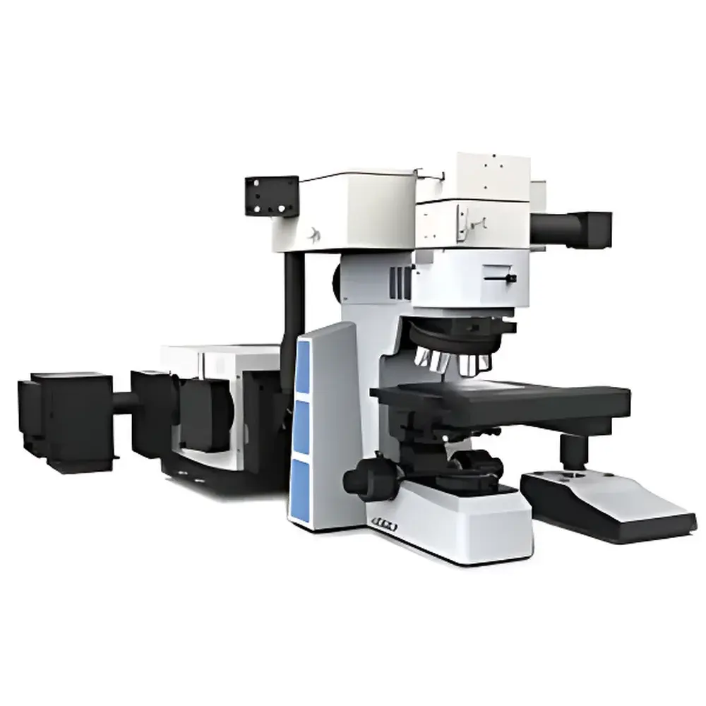
ZOLIX SPM900 Series Minority Carrier Lifetime Imaging System
| Brand | ZOLIX |
|---|---|
| Model | SPM900 |
| Origin | Beijing, China |
| Instrument Type | Time-Resolved Photoluminescence (TRPL) Microscope-Based Lifetime Imager |
| Excitation Wavelengths | 375–670 nm (ps-pulsed lasers) |
| Spectral Range | 200–900 nm |
| Minimum Temporal Resolution | 16 ps |
| Lifetime Measurement Range | 500 ps – 1 ms |
| Spatial Resolution | ≤ 1 µm (with 100× objective, 405 nm excitation) |
| Scan Area | Up to 200 × 250 mm (for 8-inch wafers) |
| TCSPC Dead Time | < 10 ns |
| Maximum Count Rate | 100 Mcps |
| Cooling | -60 °C (CCD), Peltier-cooled PMT |
| Software | OmniFluo-FM (GLP-compliant data logging, audit trail, multi-exponential decay fitting ≤ 4 components) |
Overview
The ZOLIX SPM900 Series Minority Carrier Lifetime Imaging System is a research-grade, confocal time-resolved photoluminescence (TRPL) microscope engineered for quantitative, spatially resolved measurement of minority carrier recombination dynamics in semiconductor materials. It operates on the fundamental principle that radiative recombination of photogenerated minority carriers produces time-dependent photoluminescence (PL) emission—intensity decaying exponentially with characteristic lifetime τ. By coupling picosecond-pulsed laser excitation with time-correlated single-photon counting (TCSPC), the system captures nanosecond-to-millisecond PL decay kinetics at diffraction-limited spatial resolution. This enables direct mapping of local variations in non-radiative recombination centers—such as deep-level defects, impurity complexes, dislocations, or interfacial states—that govern device performance in photovoltaics, micro-LEDs, perovskites, and compound semiconductors. Unlike steady-state PL intensity mapping, lifetime imaging decouples optical absorption and quantum efficiency effects, yielding intrinsic material quality metrics independent of excitation fluence or surface reflectivity.
Key Features
- Modular TCSPC architecture with selectable picosecond pulsed lasers (375–670 nm), including 30–75 ps FWHM options and average powers up to 4.3 mW at 50 MHz repetition rate
- High-precision motorized XY stage: 75 × 50 mm travel (50 nm step size, <1 µm repeatability) for micro-scale scanning; optional 200 × 250 mm stage for full 8-inch wafer mapping
- Research-grade upright microscope with Köhler illumination, five-position objective turret, and standard 10×/50×/100× brightfield objectives (DIC and darkfield compatible)
- 320 mm focal length imaging-corrected monochromator with triple 68 × 68 mm gratings, ±0.1 nm wavelength accuracy, and 0.0025 nm scan step resolution
- Dual detection pathways: thermoelectrically cooled UV-VIS PMT (185–900 nm) and back-illuminated deep-depletion scientific CCD (2000 × 256 pixels, -60 °C operating temperature, >95% QE)
- OmniFluo-FM software with integrated hardware control, real-time FLIM acquisition, and automated multi-exponential decay fitting (up to 4 lifetime components per pixel)
Sample Compatibility & Compliance
The SPM900 supports planar semiconductor specimens ranging from micron-scale micro-LED arrays and perovskite thin films to 200 mm (8-inch) silicon or GaAs wafers. It accommodates both conductive and insulating substrates, including Si, Ge, GaAs, InP, CdTe, ZnS, perovskites (e.g., MAPbBr₃, CsPbBr₃), and wide-bandgap nitrides. No electrical contacts or vacuum environments are required—measurements are performed under ambient or controlled N₂/Ar atmosphere. The system complies with ISO/IEC 17025 documentation requirements for calibration traceability and supports GLP/GMP-aligned workflows via timestamped, user-annotated acquisition logs, electronic signatures, and full audit trails per FDA 21 CFR Part 11 guidelines. All spectral and temporal calibrations are stored within metadata and reproducible across sessions.
Software & Data Management
OmniFluo-FM is a native Windows 10 application designed for rigorous scientific data integrity. Its acquisition module enables synchronized control of laser triggering, stage motion, detector gating, and monochromator positioning—allowing fully automated raster scans with sub-pixel dwell time optimization. The processing engine performs pixel-wise bi- or tri-exponential decay fitting using Levenberg–Marquardt nonlinear least-squares algorithms, with χ² validation and residual analysis. Outputs include parametric maps of amplitude-weighted lifetime (τₐᵥ), intensity-weighted lifetime (τᵢ), fractional amplitudes (α₁, α₂…), and goodness-of-fit metrics (R², reduced χ²). All images support histogram equalization, LUT-based pseudocoloring, contour overlays, line-profile extraction, and interactive 3D surface rendering. Raw TCSPC histograms (.ptu) and processed datasets (.h5) adhere to HDF5 standards for long-term archival and cross-platform interoperability.
Applications
- Quantitative defect density mapping in silicon PV wafers and heterojunction solar cells (e.g., passivation quality assessment of SiO₂, Al₂O₃, or poly-Si layers)
- Spatially resolved carrier dynamics in micro-LED arrays (e.g., identifying edge degradation, current crowding zones, or epitaxial nonuniformity in 80 µm GaN microdisks)
- Mechanistic studies of radiative vs. non-radiative recombination in metal-halide perovskites—correlating dual-component lifetimes (e.g., ~10 ns surface-trap vs. ~100 ns bulk-recombination) with film morphology and halide composition
- Process monitoring of III–V MBE/MOCVD growth: quantifying SRH recombination via trap-assisted Auger or Shockley–Read–Hall lifetimes in InGaAs quantum wells
- Fundamental investigation of exciton–phonon coupling, charge-transfer states, and defect migration under thermal or optical stress
FAQ
What excitation wavelengths are supported, and how is laser selection determined?
The system integrates eight factory-calibrated picosecond lasers (375–670 nm). Selection depends on material bandgap and absorption coefficient—e.g., 405 nm for GaN, 510 nm for perovskites, 635 nm for GaAs—to maximize carrier generation while minimizing thermal load or two-photon effects.
Can the SPM900 perform absolute quantum yield measurements?
No—it is optimized for lifetime kinetics, not absolute photon flux calibration. However, relative PL quantum efficiency trends can be inferred from amplitude-normalized lifetime maps when combined with calibrated reference standards.
Is vacuum or cryogenic operation supported?
The base configuration operates at ambient pressure and temperature. Optional cryostat integration (liquid nitrogen or closed-cycle) is available for low-T TRPL studies down to 10 K, with custom optical access and vibration isolation.
How does the system handle samples with strong autofluorescence or scattering backgrounds?
TCSPC gating rejects prompt scatter and short-lived background via time-window discrimination; spectral unmixing is further enabled by high-resolution monochromator selection and multi-wavelength excitation correlation analysis.
What data formats are exportable for third-party analysis?
Raw .ptu files (PicoQuant format), processed .h5 containers (HDF5), CSV tables of fitted parameters, and TIFF stacks of pseudocolor lifetime maps—all retain full metadata including instrument settings, calibration timestamps, and user annotations.


