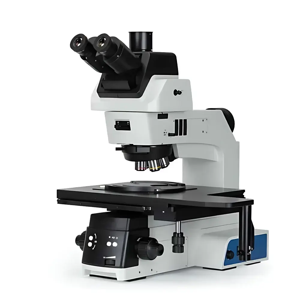
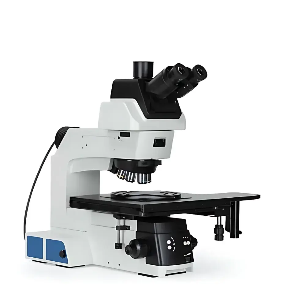
Lei-Tech LK-86R Research-Grade Upright Semiconductor & FPD Inspection Microscope
| Brand | Lei-Tech |
|---|---|
| Origin | Tianjin, China |
| Manufacturer Type | Direct Manufacturer |
| Product Type | Upright Metallurgical Microscope |
| Image Analysis System | Integrated |
| Total Magnification Range | 50×–1000× |
| Eyepiece | PL10×/23 mm |
| Objective Lenses | 5×, 10×, 20×, 50×, 100× (Brightfield/Darkfield Semi-Apochromatic Metallurgical Objectives) |
| Optical System | Infinity-Corrected UISC (Ultra-Infinity Super-Correction) |
| Observation Modes | Brightfield, Darkfield, DIC (Nomarski), Simple Polarization |
| Illumination | Reflected 12 V/100 W Halogen with Pre-Set Intensity & BF/DF Toggle |
| Focus Mechanism | Coaxial Coarse/Fine Drive (35 mm Coarse Travel, 1 µm Fine Resolution) |
| Stage | 8-inch (200 mm) Triple-Layer Mechanical Stage, 210 × 210 mm Travel, Clutch-Engaged Rapid Movement |
| Observation Tube | Ergonomic Trinocular Tube, 5°–35° Tiltable, Fixed 100:0 or 0:100 Beam Splitting |
| Vibration Damping | Six-Point Low-CG Metal Chassis with Integrated Anti-Vibration Support |
| Objective Turret | Motorized 6-Position Turret with DIC Slot & Auto-Aperture Matching |
| Software Features | Real-Time Extended Depth of Field (EFI), Multi-Image Alignment (MIA), Onboard Measurement & Annotation |
Overview
The Lei-Tech LK-86R is a research-grade upright metallurgical microscope engineered specifically for high-precision inspection of semiconductor wafers, flat panel display (FPD) substrates, and advanced optoelectronic materials. Built upon an ultra-stable, fully metallic mechanical architecture and an infinity-corrected UISC (Ultra-Infinity Super-Correction) optical pathway, the LK-86R delivers diffraction-limited resolution across its full magnification range (50×–1000×) while maintaining exceptional field flatness and chromatic fidelity. Its dual-path illumination system—combining high-intensity reflected halogen lighting (12 V/100 W) with a thermally stable transmitted white LED (5 W)—enables simultaneous or independent brightfield, darkfield, differential interference contrast (DIC), and simple polarization observation modes. Designed to accommodate substrates up to 200 mm in diameter (8-inch wafers) or 279 mm diagonally (11-inch FPD panels), the LK-86R meets the dimensional and metrological demands of front-end process control labs, failure analysis (FA) suites, and academic microstructure laboratories.
Key Features
- UISC infinity-corrected optical design ensures minimal aberration, consistent MTF performance, and compatibility with auxiliary modules including DIC prisms, polarization analyzers, and fluorescence filter cubes.
- Motorized 6-position objective turret with automatic aperture synchronization: the condenser iris dynamically adjusts to match selected objective NA, eliminating manual recalibration and ensuring repeatable Köhler illumination across magnifications.
- Ergonomic tilting trinocular observation tube (5°–35°), adjustable interpupillary distance (50–76 mm), and diopter-compensated PL10×/23 mm wide-field eyepieces reduce operator fatigue during extended inspection sessions.
- Clutch-actuated mechanical stage enables seamless transition between coarse positioning (full 210 × 210 mm travel) and fine micrometric adjustment—ideal for systematic defect mapping across large-area substrates.
- Integrated vibration-damped chassis with six-point support and low center-of-gravity geometry provides mechanical stability under ambient lab conditions, critical for high-magnification DIC and quantitative image analysis.
- Real-time EFI (Extended Focus Imaging) and MIA (Multi-Image Alignment) algorithms are embedded in the native imaging software, enabling automated depth stacking and gigapixel-scale mosaic reconstruction without external computing hardware.
Sample Compatibility & Compliance
The LK-86R supports rigid, non-transmissive specimens typical of semiconductor fabrication—including silicon wafers (4″, 6″, 8″), glass and quartz FPD substrates, metalized PCBs, MEMS devices, and ceramic packaging. Its reflective-only configuration complies with ISO 9001 manufacturing protocols and aligns with ASTM E1558 (Standard Guide for Metallographic Specimen Preparation) and SEMI F20 (Specification for Wafer Surface Inspection Equipment). While not certified to FDA 21 CFR Part 11 out-of-the-box, the system’s audit-trail-capable image acquisition software can be configured to meet GLP/GMP documentation requirements when deployed in regulated QC environments. All optical components—including semi-apochromatic objectives and DIC Wollaston prisms—undergo individual calibration verification per ISO 10110-5.
Software & Data Management
The bundled image analysis suite operates natively on Windows 10/11 and supports DIC quantitative phase gradient mapping, particle count/size distribution (per ISO 13322-2), line profile extraction, and calibrated area measurement with traceable NIST-referenced stage encoders. Raw image data is saved in TIFF (16-bit linear) or proprietary .LKM format with embedded metadata: objective ID, magnification, illumination mode, exposure time, and user-defined annotation tags. Export options include CSV for statistical reporting, PDF reports with embedded scale bars and measurement overlays, and direct DIC parameter export for cross-platform correlation with SEM or AFM datasets. The software architecture permits integration with LIMS via configurable REST API endpoints and supports role-based access control for multi-user laboratory deployments.
Applications
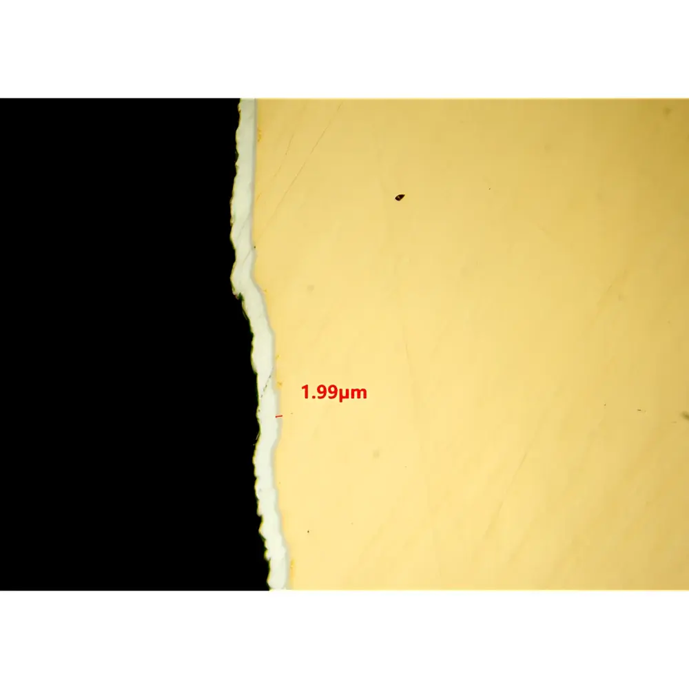
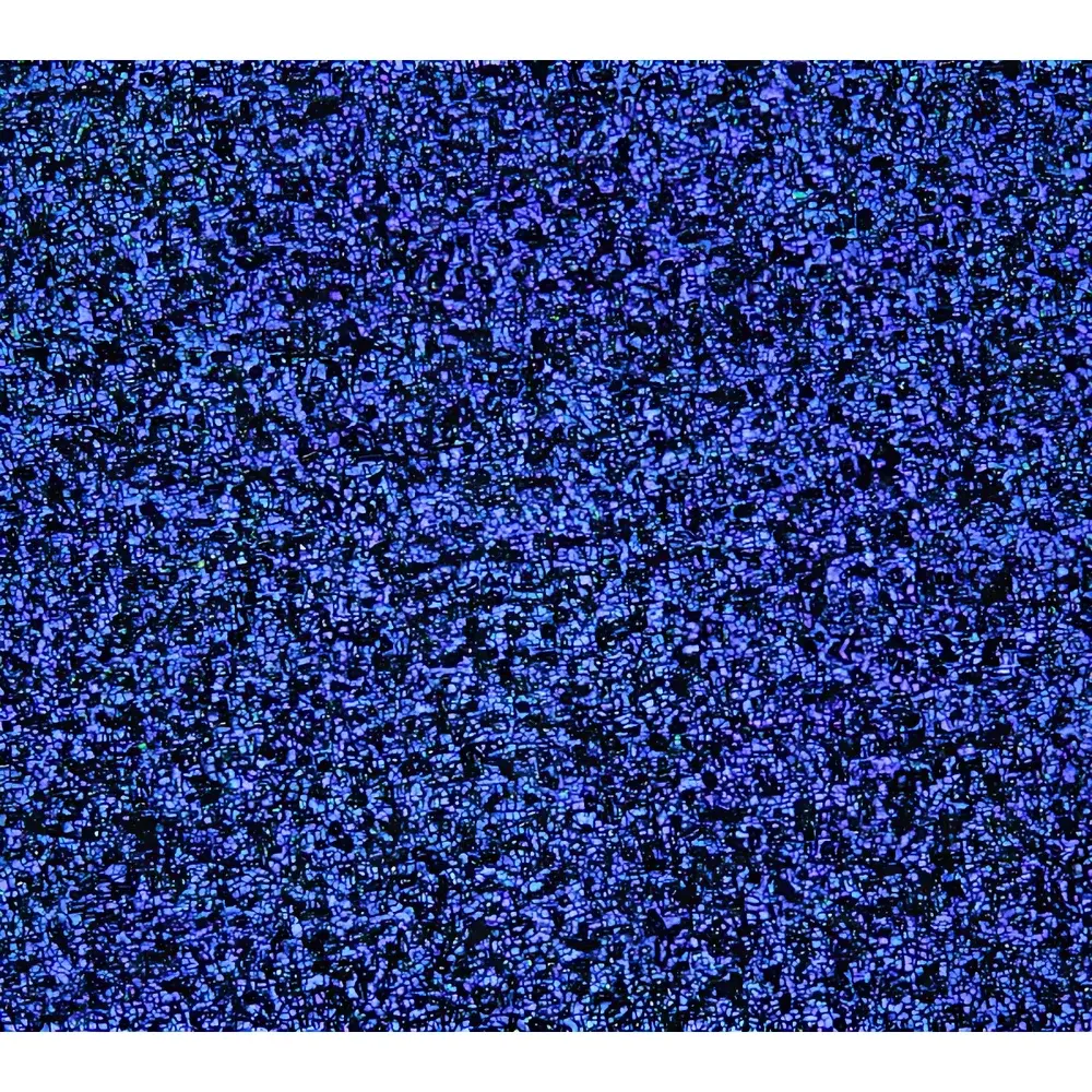
The LK-86R serves as a primary tool in wafer-level defect review (e.g., scratch detection on SiO₂ layers, particle adhesion on photoresist), FPD pixel electrode continuity verification, thin-film uniformity assessment (ITO, Mo, Al), and failure root cause analysis in power electronics packaging. Its DIC capability enables sub-100 nm topographic contrast enhancement—critical for identifying micro-cracks in GaN-on-Si epitaxial layers or edge delamination in OLED encapsulation films. In academic settings, it supports teaching and research in physical metallurgy (grain boundary characterization in Al alloys), geoscience (mineral birefringence quantification), and biomaterial surface engineering (hydroxyapatite coating roughness analysis). Routine use cases include incoming material inspection per IPC-A-600, post-etch residue evaluation, and post-CMP scratch density measurement per SEMI D38.
FAQ
Does the LK-86R support motorized Z-axis focus stacking?
Yes—the integrated EFI module performs real-time focus stacking during live acquisition using closed-loop piezo-driven objective movement with 1 µm step resolution.
Can third-party DIC accessories be mounted?
The LK-86R includes standardized DIC slots in both the objective turret and nosepiece; compatibility is confirmed for Leica, Olympus, and Nikon OEM DIC sliders meeting DIN 29232 mechanical interface specifications.
Is the transmitted LED illumination suitable for colorimetric analysis?
The 5 W white LED features a CRI >90 and spectral stability <±0.5% over 10,000 hours, making it suitable for qualitative color assessment—but not for absolute reflectance spectroscopy without external spectrometer coupling.
What is the warranty coverage and service response protocol?
Lei-Tech provides a 24-month parts-and-labor warranty with 7×24 remote diagnostics support and on-site engineer dispatch within 72 business hours in Tier-1 global markets (US, EU, Japan, Korea, Singapore).
How is calibration traceability maintained?
Each delivered system includes a factory calibration certificate referencing NIST-traceable stage encoders and photometric standards; annual recalibration services follow ISO/IEC 17025-accredited procedures at authorized service centers.


