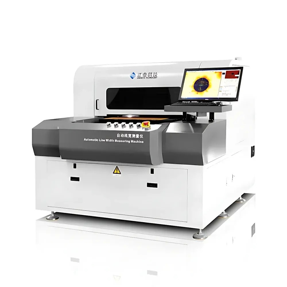
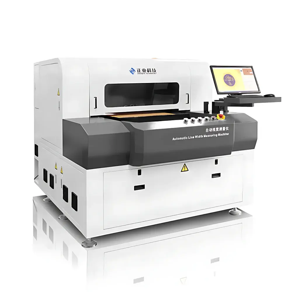
Zhengye XK32 Automated Line Width Measurement System
| Brand | Zhengye |
|---|---|
| Origin | Guangdong, China |
| Manufacturer Type | Direct Manufacturer |
| Region of Origin | Domestic (China) |
| Model | XK32 |
| Pricing | Available Upon Request |
| Dimensions (W×D×H) | 1700 mm × 2050 mm × 1600 mm |
| Weight | ~1750 kg (excluding computer) |
| Power Supply | 3-Phase AC 380 V + N + PE, 50 Hz, 5 kW |
| Operating Temperature | 20–40 °C |
| Relative Humidity | 40–70 % RH |
| Lens | Motorized Zoom Lens (0.7×–4.5×) |
| Field of View (FOV) at Magnifications | 0.7× = 3.5 mm, 1× = 3.2 mm, 2× = 2.2 mm, 3× = 1.5 mm, 4× = 1.0 mm (±5 % tolerance) |
| Line Width Measurement Range | 20 µm – 1200 µm |
| Measurement Accuracy | 1× = ±3 µm, 2× = ±2 µm, 3× = ±1 µm, 4× = ±1 µm (calibrated using certified reference standards |
| Maximum Sample Size | ≤600 mm × 650 mm |
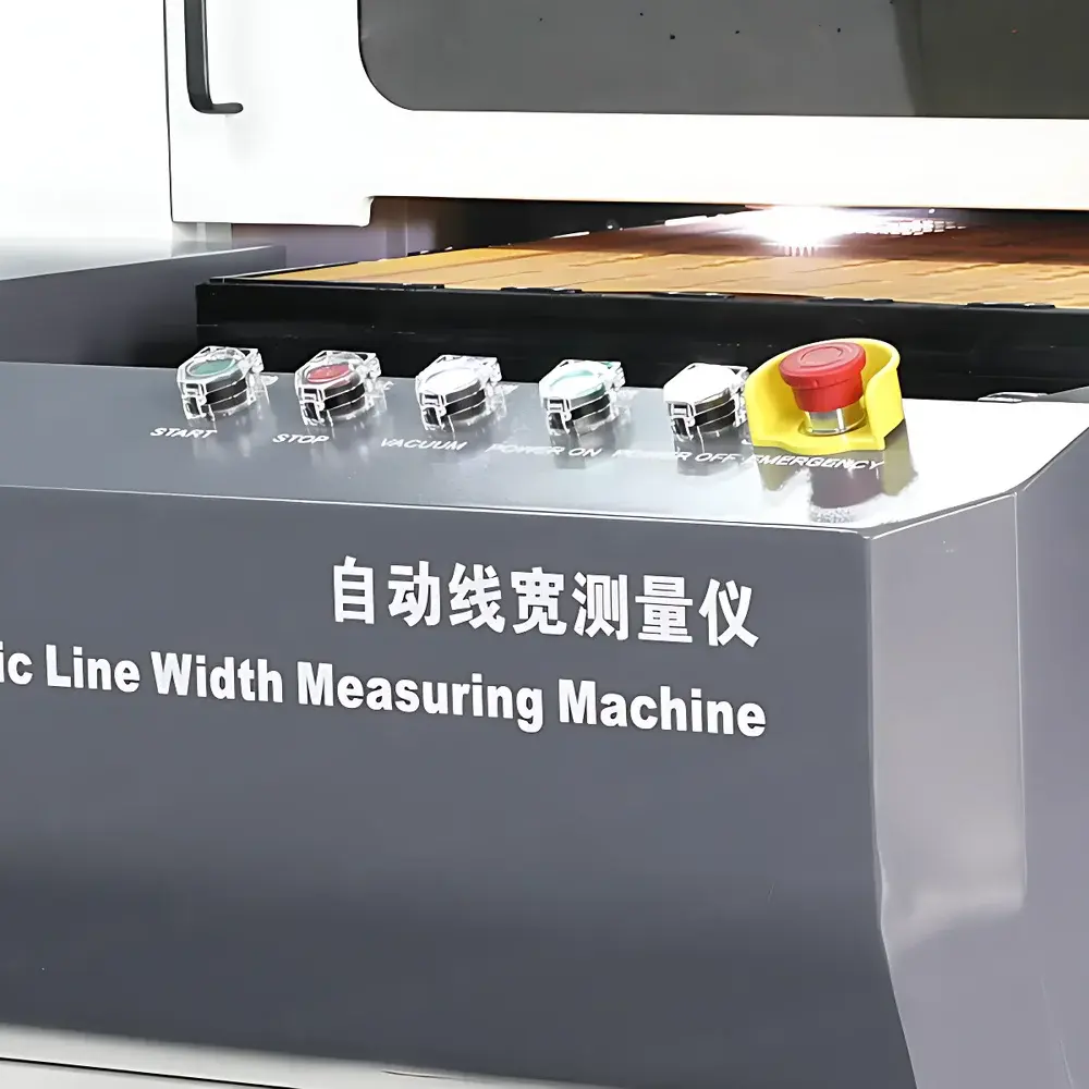
| Illumination | High-Stability LED Ring Light |
| Navigation | CCD-Based On-Screen Navigation with Real-Time Image Mapping |
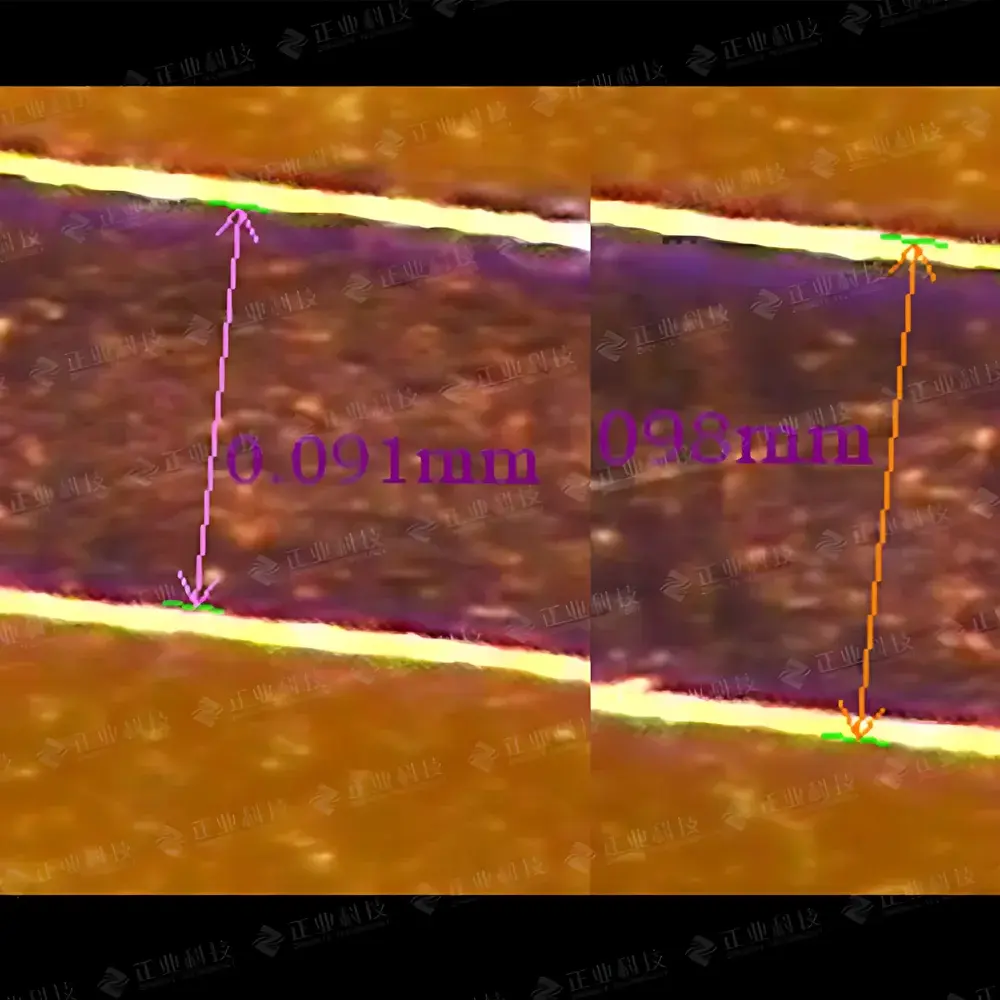
| Edge Detection | Auto-Edge Recognition (dual-edge, centerline, gap, diameter, radial symmetry) |
| Data Export | Native Excel (.xlsx) export with statistical summary (CPK, Cpk, X̄-R, histogram, trend charts) |
| Software Control | Programmable measurement sequence import/export (DXF-based coordinate referencing), batch execution with audit trail logging |
Overview
The Zhengye XK32 Automated Line Width Measurement System is a high-precision optical metrology platform engineered for non-contact, quantitative dimensional analysis of micro-scale conductive features in printed circuit board (PCB), semiconductor wafer, and flat-panel display (FPD) manufacturing processes. Built upon a robust industrial-grade mechanical architecture and integrated with a motorized zoom optical train, the system implements digital image-based metrology grounded in sub-pixel edge detection algorithms and calibrated geometric projection models. It operates on the principle of high-resolution CCD imaging coupled with controlled LED ring illumination to maximize contrast-to-noise ratio (CNR) across varying surface topographies—particularly critical for evaluating etched copper traces, solder mask openings, via pads, and LCD electrode patterns prior to subsequent process steps (e.g., solder mask application or bonding). Designed for integration into production-line quality control workflows, the XK32 delivers traceable, repeatable measurements compliant with IPC-6012, IPC-A-600, and JIS Z 8401 standards for dimensional verification in electronics fabrication.
Key Features
- DXF-Driven Programmable Metrology: Supports direct import of industry-standard DXF files to define measurement coordinates, feature types (line width, line spacing, hole diameter, edge-to-hole distance), and tolerancing—enabling rapid setup of inspection routines without manual point selection.
- Motorized Zoom Optics (0.7×–4.5×): Eliminates manual lens exchange; enables seamless, software-controlled magnification switching during automated sequences to optimize resolution vs. field-of-view trade-offs per feature size.
- Auto-Focus & Focus Stability Algorithm: Employs contrast-based iterative focus search combined with Z-axis position feedback to maintain optimal focal plane across large-area samples and thermal drift conditions.
- Real-Time CCD Navigation Interface: Provides an overview map synchronized with high-magnification measurement view, allowing operators to pan/zoom and rapidly relocate to predefined or user-marked positions.
- Sub-Pixel Edge Detection Engine: Implements gradient-thresholding and second-derivative zero-crossing methods to locate edges with repeatability better than ±0.5 pixel—critical for achieving the specified 1 µm accuracy at 3× magnification.
- Audit-Ready Data Management: All measurement sessions are timestamped, operator-tagged, and stored with full metadata (optical settings, calibration status, environmental logs); supports configurable export to Excel with statistical process control (SPC) metrics including Cp, Cpk, Pp, Ppk, and control chart generation.
Sample Compatibility & Compliance
The XK32 accommodates rigid and semi-rigid substrates up to 600 mm × 650 mm, including multilayer PCB panels (inner/outer layer post-etch, pre-solder mask), IC wafers (up to 8-inch diameter with optional carrier), and LCD glass substrates. Its optical design mitigates parallax error across the full working distance range, and the LED ring light ensures uniform illumination independent of surface reflectivity variations. The system meets CE electromagnetic compatibility (EMC) directives and conforms to ISO 17025-recommended practices for measurement uncertainty estimation. While not FDA-certified as a medical device, its data handling architecture supports 21 CFR Part 11-compliant electronic signatures and audit trails when deployed in regulated environments requiring GLP/GMP documentation integrity.
Software & Data Management
The proprietary measurement software runs on Windows OS and provides a dual-mode interface: guided wizard mode for first-time users and advanced script mode for engineering-level customization. Measurement programs—including coordinate sets, magnification profiles, lighting presets, and pass/fail logic—are saved as encrypted .xk32proj files with version control. Raw images and coordinate data are retained in lossless TIFF format alongside processed results. Statistical summaries auto-generate histograms, capability indices, and time-series plots. Data exports include both raw tabular output (.xlsx) and PDF reports with embedded annotations, calibration certificates, and measurement uncertainty statements aligned with GUM (Guide to the Expression of Uncertainty in Measurement) principles.
Applications
- PCB Fabrication: Quantitative assessment of line width uniformity (LWU), line edge roughness (LER) proxy, conductor spacing (pitch), annular ring integrity, and drill-to-copper registration.
- Semiconductor Packaging: Verification of redistribution layer (RDL) trace geometry, bump pad dimensions, and scribe lane widths on interposers and fan-out wafers.
- Display Manufacturing: Measurement of TFT gate/data line widths, black matrix openings, and touch sensor electrode pitch on TFT-LCD and OLED substrates.
- Quality Auditing: First-article inspection (FAI), in-process verification (IPV), and final acceptance testing (FAT) per customer-specific AQL sampling plans.
- Process Development: Correlation of etch parameters (chemistry, time, temperature) with dimensional outcomes via longitudinal measurement datasets.
FAQ
What calibration standards are supported for traceability?
The XK32 is supplied with NIST-traceable line width calibration standards (chrome-on-glass photomasks) certified to ±0.1 µm uncertainty. Users may perform in-house calibration verification using these artifacts at designated magnifications.
Can the system integrate with factory MES or SPC platforms?
Yes—via TCP/IP socket communication and configurable CSV/Excel export templates, the XK32 supports bidirectional data exchange with common MES (e.g., Siemens Opcenter, Camstar) and SPC systems (e.g., InfinityQS, Minitab Workspace).
Is environmental conditioning required for operation?
While the system operates within 20–40 °C and 40–70 % RH, optimal measurement stability is achieved in temperature-controlled rooms (±1 °C/hour drift) with anti-vibration flooring—especially when targeting sub-2 µm repeatability.
How is measurement uncertainty quantified and reported?
Uncertainty budgets are calculated per ISO/IEC 17025 Annex A, incorporating contributions from optical magnification error, stage positioning repeatability, edge detection algorithm variance, and environmental thermal expansion coefficients—reported in all PDF certificates.
Does the software support multi-user role-based access control?
Yes—administrator, engineer, and operator roles are enforced with password protection, activity logging, and granular permissions for program editing, calibration access, and report generation.


