PCB Gold-Nickel Coating Thickness Analyzer (XRF-based, Energy-Dispersive)
| Origin | UK |
|---|---|
| Manufacturer Type | Authorized Distributor |
| Origin Category | Imported Instrument |
| Model | XDV-SDD |
| Price Range | USD 27,000 – 68,000 |
Overview
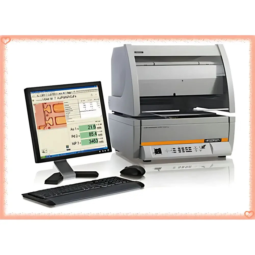
The XDV-SDD is a high-performance energy-dispersive X-ray fluorescence (ED-XRF) coating thickness analyzer engineered specifically for non-destructive, quantitative measurement of ultra-thin metallic layers on printed circuit boards (PCBs) and other microelectronics substrates. Operating on the fundamental principle of characteristic X-ray emission induced by primary X-ray excitation, the system enables precise determination of gold (Au), nickel (Ni), palladium (Pd), copper (Cu), tin (Sn), and other elemental coatings—down to sub-100 nm thicknesses—without sample preparation or physical contact. Its core architecture integrates a high-resolution silicon drift detector (SDD), optimized X-ray tube optics, and a motorized XYZ stage with programmable positioning accuracy of ±1 µm, ensuring repeatable analysis across complex PCB geometries including fine-pitch pads, edge connectors, and multi-layer vias.
Key Features
- Energy-dispersive XRF detection with <125 eV Mn-Kα resolution at 100,000 cps, enabling robust spectral deconvolution of overlapping peaks (e.g., Ni Kα/Ni Kβ, Au L-lines/Sn K-lines)
- Motorized, software-controlled X/Y/Z stage with 200 × 200 mm travel range and automated pattern recognition for batch mapping of up to 999 measurement points per sample
- Calibration traceable to NIST SRM reference standards; supports both fundamental parameter (FP) and empirical calibration modes for multi-layer systems
- Integrated helium purge path for enhanced light-element sensitivity (e.g., P, S, Cl) required for RoHS-compliant halogen screening
- Rugged industrial enclosure rated IP54, designed for integration into QC labs and pilot production lines with minimal environmental conditioning
- Compliance-ready firmware supporting audit trails, user access levels, and electronic signature workflows aligned with ISO/IEC 17025 and IATF 16949 quality management requirements
Sample Compatibility & Compliance
The XDV-SDD accommodates standard PCB formats up to 305 × 305 mm (12″ × 12″) and accepts rigid, flex, and rigid-flex substrates with surface warpage ≤0.5 mm. It supports direct analysis of solder mask-covered areas, ENIG (electroless nickel immersion gold), ENEPIG, immersion silver, and OSP-coated surfaces without masking or etching. All measurement protocols are compatible with IPC-4552A (ENIG), IPC-4556 (ENEPIG), and ASTM B568–98(2022) for XRF-based coating thickness determination. Data output meets GLP/GMP documentation standards, including full spectral archives, measurement metadata (voltage, current, live time, geometry), and uncertainty estimation per ISO 14707.
Software & Data Management
Controlled via the proprietary ThincPro v4.2 platform, the system delivers intuitive workflow management—from method setup and calibration validation to statistical process control (SPC) charting. Software modules include Multi-Layer Solver for simultaneous quantification of up to five stacked layers (e.g., Cu/Ni/Au or Cu/Pd/Ni/Au), RoHS Quantifier for restricted substance screening against EU Directive 2011/65/EU limits, and Auto-Report Generator compliant with FDA 21 CFR Part 11 for electronic records and signatures. Raw spectra and processed results are stored in vendor-neutral .csv and .dxp formats; optional SQL database integration enables centralized data warehousing and cross-instrument trending.
Applications
- Quantitative thickness verification of immersion gold (0.03–0.2 µm) and electroless nickel (2–8 µm) in ENIG finishes per IPC-4552A
- Trace-level detection of Cd, Pb, Hg, Cr(VI), and Br in solder masks and component terminations for RoHS/WEEE compliance verification
- Composition analysis of wire-bondable gold plating (≥99.99% purity) and functional barrier layers in advanced packaging substrates
- Process validation of selective plating steps in HDI and IC substrate manufacturing
- Failure analysis support for corrosion-induced delamination, intermetallic growth, and under-plating voids via depth-profiling mode
- Automated SPC monitoring of plating bath performance using trended thickness and alloy ratio (Ni:P) metrics
FAQ
Does the XDV-SDD require radioactive sources or vacuum operation?
No. It uses a sealed-end-window X-ray tube (50 kV, 1 mA max) and operates under ambient air or helium atmosphere—no isotopic sources or high-vacuum pumps are required.
Can it measure nickel phosphorus (Ni-P) composition in electroless nickel deposits?
Yes. The SDD’s light-element sensitivity and FP algorithm enable quantification of phosphorus content (1–12 wt%) alongside Ni thickness, critical for assessing corrosion resistance and solderability.
Is method transfer possible between different XDV-SDD units?
Yes. Calibration files—including detector response curves, geometry corrections, and matrix correction coefficients—are fully portable across instruments within the same hardware generation.
What maintenance is required beyond annual calibration?
Routine maintenance is limited to X-ray tube lifetime monitoring (typically >20,000 hours), SDD window inspection, and stage lubrication every 12 months—no optical alignment or detector cooling refills are needed.
Does the system support custom reporting for internal QA documentation?
Yes. ThincPro includes a template editor supporting company-specific headers, logo insertion, approval workflows, and export to PDF/A-2b for long-term archival compliance.
Related Products


