Zhengye X-ray Inspection System for IGBT Module Non-destructive Testing
| Brand | Zhengye |
|---|---|
| Origin | Guangdong, China |
| Manufacturer Type | OEM/ODM Manufacturer |
| Country of Origin | China |
| Model | Zhengye X-ray Inspection Machine |
| Pricing | Available Upon Request |
Overview
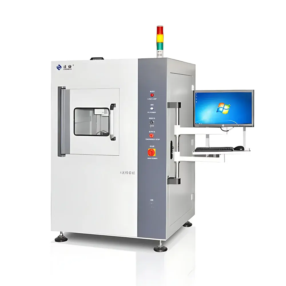
The Zhengye X-ray Inspection System for IGBT Module Non-destructive Testing is an industrial-grade, real-time radiographic imaging platform engineered for high-precision internal structural analysis of power semiconductor modules. Based on the principle of X-ray transmission radiography, the system generates high-contrast grayscale images by measuring differential attenuation of X-ray photons as they pass through materials of varying density and atomic composition. This enables non-invasive visualization of solder joint integrity, wire bond continuity, die attach voids, delamination, cracking, and interconnect misalignment—critical failure modes in insulated-gate bipolar transistor (IGBT) modules used in EV inverters, renewable energy converters, and industrial motor drives. Unlike destructive cross-sectioning or time-intensive acoustic microscopy, this system delivers immediate, repeatable, and traceable inspection results without compromising device functionality or reliability.
Key Features
- CNC Programmable Motion Control: Integrated three-axis (X/Y/Z) motion architecture for X-ray source and image intensifier, driven by precision stepper motors and guided by ground-rolled ball screws and synchronous timing belts—ensuring sub-micron repeatability and smooth positional stability during sequential inspections.
- Intelligent Navigation & Target Localization: Large-format live navigation window overlays real-time radiographic preview with coordinate mapping; click-to-move functionality enables instantaneous repositioning to any region of interest (ROI) with automated stage recalibration.
- Automated Defect Recognition Software: Proprietary image analysis suite supports rule-based thresholding, edge detection, and comparative template matching—enabling autonomous measurement of bond length, void area percentage, solder thickness uniformity, and lead frame alignment deviation. Pass/fail classification is displayed in a dedicated result interface with timestamped audit logs.
- Real-Time Image Processing Engine: Supports DICOM, TIFF, BMP, and PNG export formats; includes dynamic range compression, contrast enhancement, noise suppression, and geometric distortion correction algorithms optimized for low-dose, high-resolution radiography of multi-layered ceramic substrates and copper-aluminum metallization stacks.
- Modular Mechanical Design: Fixed sample stage accommodates standard IGBT module footprints (up to 150 mm × 120 mm); independent X-ray tube and image intensifier movement eliminates parallax error and enables oblique-angle tomographic scanning capability when configured with rotational accessories.
Sample Compatibility & Compliance
The system is validated for inspection of press-pack and solder-bonded IGBT modules incorporating Si or SiC dies, DBC (Direct Bonded Copper) or AMB (Active Metal Brazed) substrates, and Al or Cu wire bonds (25–500 µm diameter). It complies with IEC 61000-6-3 (EMC emissions), IEC 61000-6-4 (industrial immunity), and meets mechanical safety requirements per ISO 13857. While not certified as a medical device, its radiation shielding design conforms to national Class II X-ray equipment regulations (CNCA-C11-01:2023) and incorporates interlocked access doors, dose monitoring sensors, and automatic beam shutdown upon door opening. Optional integration with factory MES systems supports traceability aligned with ISO 9001:2015 and IATF 16949 quality management frameworks.
Software & Data Management
The embedded inspection software provides full GLP-compliant data handling: all images, measurement parameters, operator IDs, timestamps, and pass/fail decisions are stored in encrypted SQLite databases with configurable retention policies. Audit trail functionality records every user action—including parameter modification, ROI adjustment, and report generation—in accordance with FDA 21 CFR Part 11 requirements for electronic records and signatures. Export options include CSV-formatted metrology reports, annotated image sequences, and PDF inspection certificates compatible with SPC (Statistical Process Control) platforms. Remote diagnostics and firmware updates are supported via secure HTTPS API endpoints.
Applications
- Failure analysis of IGBT modules post-temperature cycling or power cycling stress tests
- In-process verification of die attach quality during module assembly line integration
- Root cause identification of short-circuit failures in traction inverters
- Qualification testing of new substrate materials (e.g., SiC-on-Si vs. SiC-on-SiC)
- Comparative evaluation of solder paste reflow profiles across thermal profiles
- Support for AEC-Q101 qualification documentation packages
FAQ
What X-ray energy range does this system operate within?
The system utilizes a microfocus X-ray tube with adjustable kV settings from 40 kV to 130 kV, optimized for penetration of aluminum housings, ceramic substrates, and copper busbars typical in automotive-grade IGBT modules.
Is the software compliant with FDA 21 CFR Part 11?
Yes—the software implements role-based access control, electronic signature workflows, and immutable audit trails required for regulated environments including automotive Tier-1 suppliers undergoing AIAG VDA audits.
Can the system perform quantitative void analysis on solder joints?
Yes—using calibrated grayscale thresholds and pixel-area mapping, the software calculates void fraction (%) relative to total solder joint area, with measurement uncertainty traceable to NIST-traceable reference phantoms.
Does it support offline analysis of captured images?
Yes—exported image files retain full bit-depth metadata and can be imported into third-party metrology tools (e.g., ImageJ, MATLAB, or commercial CT reconstruction suites) for advanced defect characterization.
What is the maximum sample height clearance?
The Z-axis travel allows up to 120 mm vertical clearance between detector and X-ray source, accommodating stacked dual-side cooled IGBT modules with heatsink interfaces.


