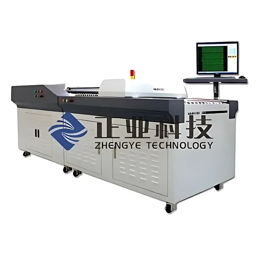
Aisida JK2400 Pore Count and Diameter Inspection System for PCBs
| Brand | Aisida |
|---|---|
| Model | JK2400 |
| Measurement Principle | Contactless CIS-based optical imaging with diffuse LED illumination |
| Pore Diameter Range | 0.10–10.0 mm |
| PCB Size Capacity | 120 × 64 mm to 610 × 610 mm |
| PCB Thickness Range | 0.08–10 mm |
| Max. Hole Count per Scan | 600,000 |
| Inspection Speed | 4.2 m/min |
| Diameter Measurement Accuracy | ≤21 µm |
| Tolerance Specification | ±50 µm |
| Imaging Method | Proximity CIS line-scan sensor with short-focus lens |
| Light Source | Diffuse linear LED array |
| Power Supply | 220 V AC, 15 A, 3 kW |
| Compressed Air Requirement | 0.6 MPa |
| Dimensions (L×W×H) | 4050 × 1280 × 1220 mm |
| Weight | 450 kg |
| Data Storage | Integrated relational database with timestamped audit trail |
| Communication Interface | CAN bus architecture |
| Compliance Framework | Designed for integration into ISO 9001-certified PCB manufacturing lines |
Overview
The Aisida JK2400 Pore Count and Diameter Inspection System is a high-throughput, non-contact optical inspection platform engineered specifically for post-drilling quality assurance in rigid and flexible printed circuit board (PCB) production. It employs a calibrated contact-imaging sensor (CIS) line-scan architecture combined with a uniform, diffuse linear LED illumination source to capture high-fidelity grayscale profiles across the entire board surface. Unlike traditional fluorescent-lamp-based systems, the JK2400’s optimized optical path—featuring a short-focus lens and precisely controlled working distance—minimizes parallax error and enhances edge contrast for sub-25 µm diameter resolution. The system operates on the principle of pixel-intensity thresholding and centroid-based geometric reconstruction, enabling deterministic identification and metrological characterization of drilled through-holes, microvias, and buried vias without physical contact or vacuum fixation. Its primary function is to verify hole count completeness, detect missing or misdrilled holes, and quantify actual diameters against nominal specifications—thereby serving as a critical gatekeeper before final packaging and shipment.
Key Features
- Diffuse linear LED illumination module providing uniform, flicker-free, long-lifetime illumination—eliminating shadow artifacts and thermal drift associated with fluorescent tubes.
- Real-time velocity-compensated algorithm that decouples measurement accuracy from conveyor speed variations, ensuring consistent repeatability across operational speeds up to 4.2 m/min.
- Short-focus optical assembly optimized for proximity CIS scanning, delivering enhanced depth-of-field control and improved lateral resolution at the board surface.
- Modular mechanical and electronic architecture: CIS sensor modules are field-replaceable, enabling hardware upgrades without full system revalidation.
- Robust pore recognition engine capable of detecting and classifying >600,000 holes per panel, including clustered, overlapping, and irregularly spaced features.
- Intelligent aperture filtering: automatic suppression of non-circular features (e.g., slots, fiducials, tool marks) based on aspect ratio and moment-of-inertia thresholds.
- CAN bus communication backbone compliant with ISO 11898-2, supporting deterministic latency, electromagnetic resilience, and seamless integration with factory automation systems (MES/SCADA).
- Built-in SQL-based relational database with encrypted storage, user-access controls, and time-stamped audit logs—supporting traceability requirements under ISO 9001 and IPC-A-600.
- Adaptive inspection mode that dynamically adjusts exposure time and gain based on substrate reflectivity and copper finish (HASL, ENIG, OSP).
Sample Compatibility & Compliance
The JK2400 accommodates standard rigid FR-4, high-Tg laminates, polyimide flex boards, and metal-core PCBs within thicknesses ranging from 0.08 mm to 10 mm. Its mechanical design supports both bare and solder-masked panels, with optional vacuum-assisted stabilization for ultra-thin (<0.2 mm) substrates. All measurement outputs—including hole count, positional coordinates (X/Y), diameter distribution histograms, and pass/fail flags—are exportable in CSV, XML, and IPC-2581 formats. The system is engineered to support quality management frameworks aligned with IPC-6012, IPC-A-600, and ISO/IEC 17025 laboratory accreditation criteria. While not FDA-regulated, its data integrity architecture—including immutable audit trails, electronic signatures, and role-based permissions—facilitates adoption in environments governed by GLP or internal QA protocols requiring documented evidence of measurement reliability.
Software & Data Management
The JK2400 runs on a real-time Linux-based embedded OS with a Qt-based GUI interface accessible via touchscreen or remote VNC. Calibration routines include automated flat-field correction, multi-point diameter reference validation using NIST-traceable gauge blocks, and dynamic focus calibration. Measurement data is stored locally in an SQLite3 database with daily auto-backup to network shares (SMB/NFS). Each inspection record contains raw image thumbnails, processed feature vectors, operator ID, timestamp, machine ID, and environmental metadata (ambient temperature/humidity if external sensors are integrated). Export modules support direct feed to statistical process control (SPC) platforms such as Minitab or InfinityQS, and RESTful API endpoints allow programmatic access for custom MES integration. All software updates are digitally signed and version-locked to prevent unauthorized modification.
Applications
- Final verification of drill accuracy prior to electroplating or solder mask application.
- Statistical analysis of drill bit wear via longitudinal diameter trend monitoring across consecutive panels.
- Root-cause analysis of hole misregistration or breakout incidents using coordinate deviation heatmaps.
- Validation of laser-drilled microvia formation consistency in HDI and IC substrate manufacturing.
- Supporting PPAP documentation packages for Tier-1 automotive electronics suppliers.
- Enabling closed-loop feedback to CNC drilling machines via OPC UA or Modbus TCP interfaces.
FAQ
What types of PCB substrates can the JK2400 inspect?
It supports rigid FR-4, high-frequency laminates (e.g., Rogers RO4000), polyimide flex, and aluminum/copper base metal-core boards—provided thickness falls within 0.08–10 mm and surface reflectivity remains within calibrated range.
Does the system require periodic recalibration?
Yes. A full optical and dimensional calibration is recommended every 200 operational hours or quarterly—whichever occurs first—using certified reference standards traceable to national metrology institutes.
Can inspection results be integrated with our existing MES?
Yes. Native support for OPC UA, Modbus TCP, and HTTP REST APIs enables bidirectional data exchange with major MES platforms including Siemens Opcenter, Rockwell FactoryTalk, and GE Digital Proficy.
Is the database exportable for long-term archival?
All records are stored in open-format SQLite3 files with schema documentation provided; exports can be scheduled automatically to network locations in CSV or XML with configurable retention policies.
What safety certifications does the JK2400 hold?
It complies with CE marking requirements (EMC Directive 2014/30/EU and Machinery Directive 2006/42/EC), and meets UL 61010-1:2012 for electrical safety in industrial measurement equipment.


