X-ray Void Inspection System for Semiconductor IC Packages
| Brand | Zhengye |
|---|---|
| Origin | Guangdong, China |
| Manufacturer Type | OEM/ODM Producer |
| Product Category | Domestic Industrial X-ray Inspection Equipment |
| Model | X-Ray Void Inspector Series |
| Pricing | Available Upon Request |
Overview
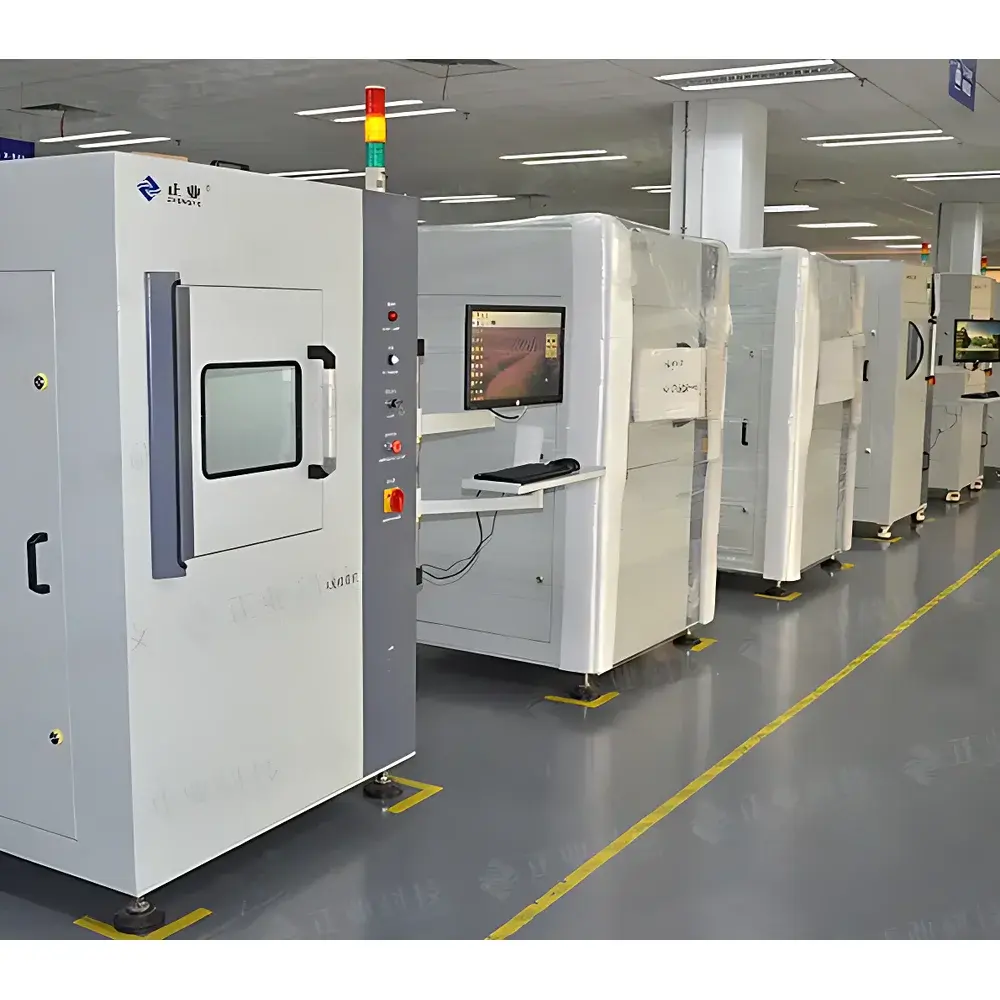
The Zhengye X-ray Void Inspection System for Semiconductor IC Packages is an industrial-grade non-destructive testing (NDT) platform engineered for high-precision internal defect analysis of microelectronic packaging structures. Leveraging digital radiography based on X-ray transmission physics, the system generates high-contrast grayscale projection images by differentiating material density and thickness variations within packaged chips, bond wires, solder joints, and underfill layers. Unlike conventional 2D X-ray systems limited to planar interpretation, this platform supports calibrated 2.5D metrology—enabling quantitative depth-aware measurements such as void area ratio, delamination extent, and solder ball height estimation through multi-angle image correlation and geometric calibration. Designed specifically for post-packaging quality assurance in semiconductor assembly lines, it meets the functional requirements of failure analysis (FA) labs, incoming quality control (IQC), and reliability screening workflows where detection of sub-100 µm voids in copper pillars, BGA substrates, or stacked-die configurations is critical.
Key Features
- 2.5D Metrological Capability: Supports calibrated linear distance, circle diameter, concentricity, and point-to-center measurements with pixel-level spatial registration; enables cross-sectional inference via Z-axis motion-coupled image stacking.
- CNC Path Programming: Stores and repeats complex inspection trajectories with sub-micron repeatability; ideal for batch validation of identical IC packages without manual repositioning.
- Real-time Navigation Interface: Features a large-field-of-view (FOV) navigation window synchronized with high-resolution detector output; click-to-move functionality allows instant translation to any coordinate within the image space with closed-loop servo feedback.
- Digital Image Processing Engine: Native support for DICOM, TIFF, PNG, and BMP formats; includes real-time contrast enhancement, noise suppression, edge sharpening, and histogram equalization algorithms optimized for low-dose radiographic imaging.
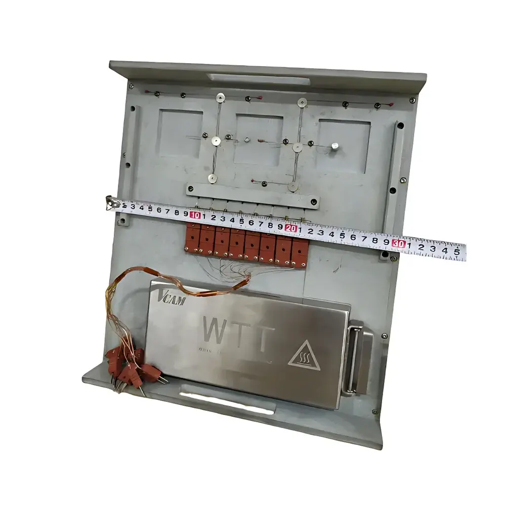
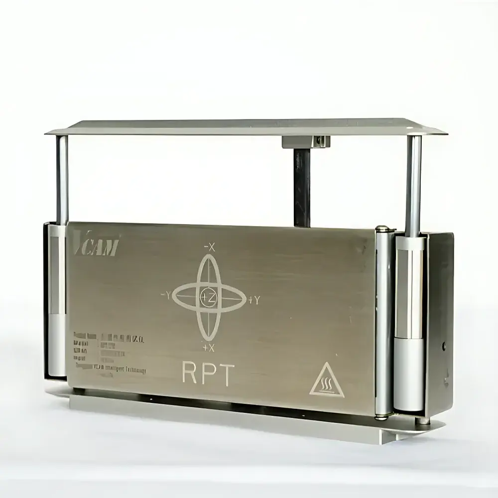
- Triaxial Motion Architecture: Independent motorized control of X-ray tube (source), image intensifier/detector (receiver), and sample stage along X, Y, and Z axes; precision movement achieved via ground-accuracy ball screws and synchronous belt-driven stepper motors with position encoders.
Sample Compatibility & Compliance
The system accommodates standard JEDEC trays (up to 330 × 280 mm), bare dies (down to 0.5 mm × 0.5 mm), and fully assembled modules including QFN, BGA, WLCSP, and SiP packages. Sample mounting uses vacuum-assisted fixtures compatible with thermal expansion compensation during extended dwell-time inspections. While not certified to ISO 17025 or accredited per IEC 62471, the platform complies with GB/T 19001–2016 (equivalent to ISO 9001:2015) for manufacturing process control and adheres to national Chinese safety standards for Class II X-ray equipment (GBZ 138–2002). Optional radiation shielding enclosures meet local occupational exposure limits (<1 µSv/h at 5 cm from cabinet surface).
Software & Data Management
The proprietary Zhengye X-ray Analysis Suite (v4.2+) provides automated void detection using adaptive threshold segmentation and morphological filtering. Measurement results—including void count, maximum void area, centroid offset, and circularity index—are exported in CSV/Excel format with timestamped audit trails. The software maintains full traceability per inspection session, recording operator ID, acquisition parameters (kV/mA/exposure time), motion path logs, and user annotations. For regulated environments, optional FDA 21 CFR Part 11-compliant modules are available upon request, delivering electronic signature capability, role-based access control, and immutable data archiving aligned with GLP/GMP documentation practices.
Applications
- Void quantification in solder bumps and microbumps of advanced packaging (e.g., 2.5D/3D IC interposers)
- Delamination mapping beneath die attach layers in power modules and RF packages
- Wire bond integrity assessment—including lift-off, necking, and heel cracking detection
- Underfill coverage uniformity verification in flip-chip assemblies
- Failure root cause analysis following thermal cycling or mechanical shock testing
- Process capability studies for reflow profile optimization in SMT lines
FAQ
What is the minimum detectable void size under standard operating conditions?
Typical resolution limit is ~5–8 µm at optimal magnification (geometric unsharpness governed by focal spot size and source-to-object distance); actual detectability depends on material composition, thickness, and contrast-to-noise ratio.
Does the system support automatic pass/fail classification based on void area thresholds?
Yes—the software allows configurable rule-based decision logic (e.g., “reject if total void area > 0.02 mm² per bump”) with visual overlay and exportable binary classification reports.
Is remote operation or integration with factory MES possible?
The system supports Ethernet-based TCP/IP communication and offers OPC UA-compatible APIs for integration into Industry 4.0 architectures, enabling trigger-based inspection initiation and result push to central databases.
Can the platform be upgraded for computed tomography (CT) reconstruction?
No—this is a dedicated 2D/2.5D radiographic system; CT functionality requires rotational gantry mechanics, dual-axis tilt stages, and dedicated reconstruction firmware not included in this configuration.


")