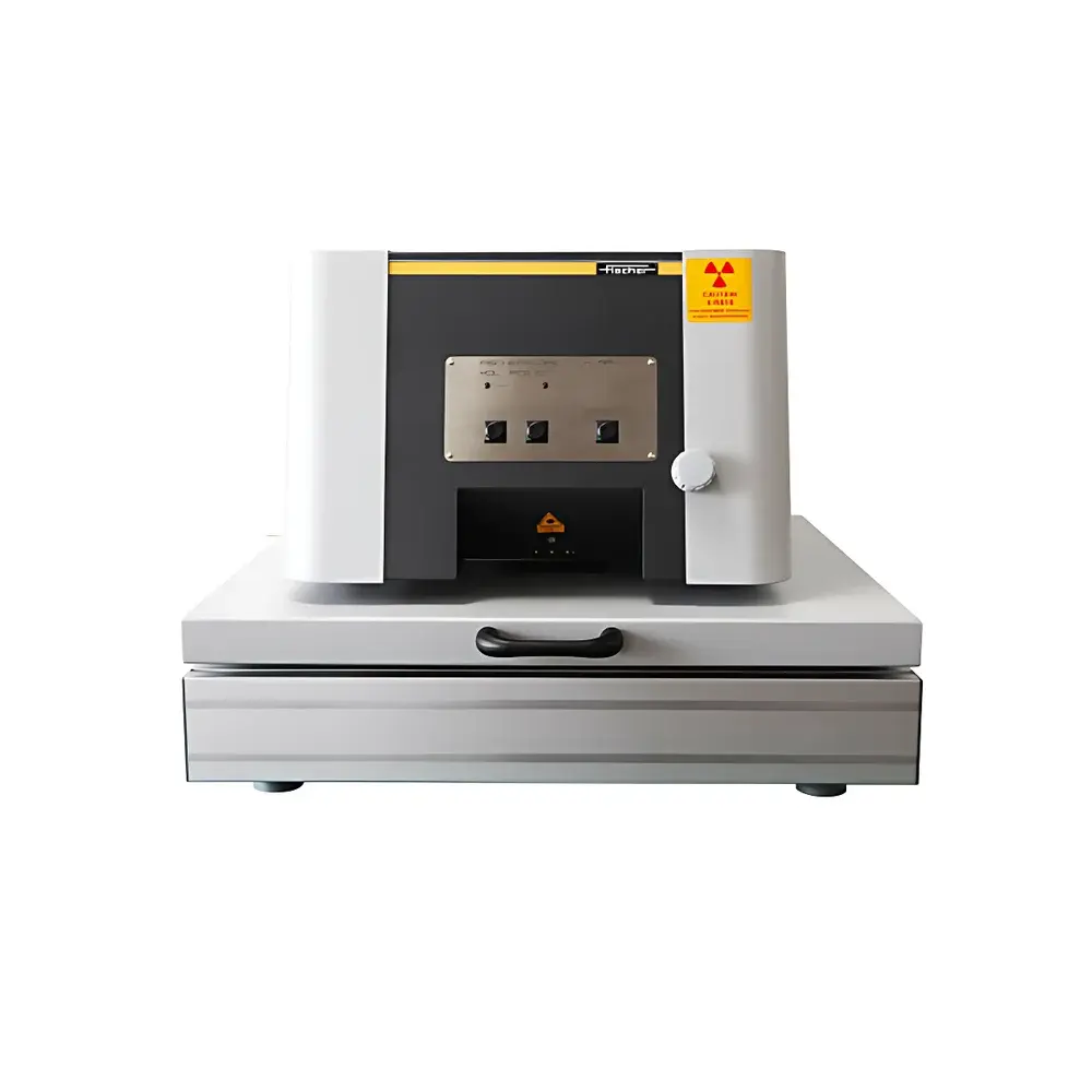
FISCHERSCOPE X-RAY ADLM-PCB Benchtop X-Ray Fluorescence Coating Thickness Analyzer
| Origin | Germany |
|---|---|
| Manufacturer Type | Authorized Distributor |
| Origin Category | Imported |
| Model | ADLM-PCB |
| Pricing | Available Upon Request |
Overview
The FISCHERSCOPE® X-RAY ADLM-PCB is a benchtop energy-dispersive X-ray fluorescence (EDXRF) analyzer engineered for non-destructive, high-precision measurement of metallic coating thicknesses—particularly gold (Au) and nickel (Ni) layers—on printed circuit boards (PCBs), connectors, contacts, and other micro-electronic or precision-engineered components. Operating on the fundamental principle of X-ray fluorescence spectroscopy, the instrument irradiates the sample with a focused X-ray beam, inducing characteristic secondary X-ray emissions from constituent elements. By quantifying the intensity ratio between the fluorescent signal from the coating and the substrate (or underlying layer), the system calculates coating thickness with trace-level sensitivity and sub-micrometer resolution. Designed specifically for electronics manufacturing and quality assurance environments, the ADLM-PCB series delivers metrological traceability aligned with international standards for coating verification and elemental composition analysis.
Key Features
- Benchtop EDXRF architecture with integrated radiation shielding and interlocked safety door—compliant with IEC 61010-1 and EU Directive 2013/59/Euratom.
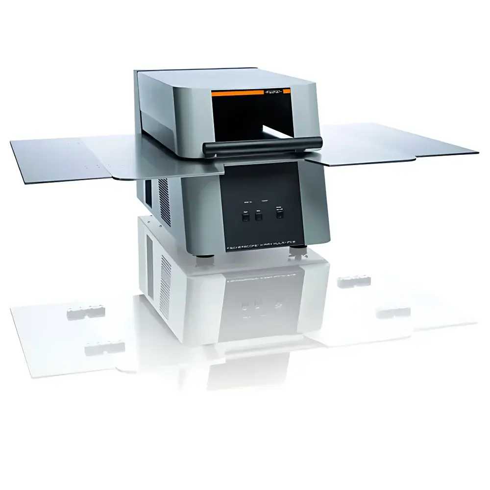
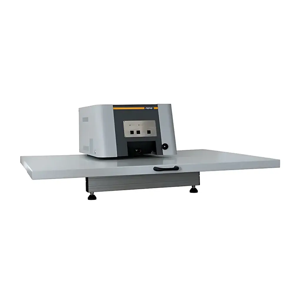
- Optimized geometry for PCB inspection: elevated measurement chamber floor clearance enables unobstructed placement of large-format PCBs up to 400 × 300 mm (ADLM-PCB 210/220 models).
- Two-stage positioning system: ADLM-PCB 200 utilizes an integrated laser crosshair and drawer-style sample stage; ADLM-PCB 210/220 integrate a motorized, programmable XY translation stage with auto-retract function and real-time visual feedback.
- High-resolution color CCD camera (≥1.3 MP) coupled with on-screen overlay of measurement spot and beam footprint—enabling precise targeting of features as small as 50 µm in diameter.
- Multi-element capability: simultaneous quantitative analysis of elements from chlorine (Z = 17) to uranium (Z = 92); up to 24 elements per measurement cycle.
- Robust mechanical design with temperature-stabilized X-ray tube and Peltier-cooled silicon drift detector (SDD) for long-term spectral stability and low detection limits (e.g., <0.01 µg/cm² for Au on Ni/Cu substrates).
Sample Compatibility & Compliance
The ADLM-PCB series accommodates flat, rigid, and moderately curved samples—including bare and solder-masked PCBs, stamped metal contacts, wire bond pads, electroplated fasteners, and thin-film semiconductor interconnects. Sample height tolerance ranges from 0 to 80 mm (depending on model and collimator configuration). All instruments are certified to DIN ISO 3497 (Metallic coatings — Measurement of coating thickness — X-ray spectrometric methods) and ASTM B568 (Standard Test Method for Thickness Measurement of Metallic Coatings by X-Ray Spectrometry), ensuring data integrity for internal QA, customer audits, and third-party certification. The system supports GLP-compliant operation via user access control, electronic signature, and full audit trail functionality within WINFTM® software—fully aligned with FDA 21 CFR Part 11 requirements for regulated industries.
Software & Data Management
Controlled exclusively via WINFTM®—FISCHER’s proprietary Windows-based analytical platform—the ADLM-PCB integrates measurement setup, calibration management, multi-point mapping, statistical process control (SPC), and report generation into a single workflow. Calibration curves support both fundamental parameters (FP) and empirical (standard-based) quantification modes. Batch measurement sequences can be programmed with position offsets, dwell times, and pass/fail thresholds. Raw spectra, peak deconvolution results, thickness maps, and trend charts are stored in vendor-neutral formats (CSV, XML, PDF) and exportable to LIMS or MES systems. Version-controlled method files ensure reproducibility across shifts and laboratories.
Applications
- Quantitative thickness verification of ENIG (electroless nickel immersion gold), ENEPIG, and flash gold plating on PCB surface finishes.
- Quality control of connector contact plating (Ni underlayer + Au topcoat) in automotive and telecom applications.
- Elemental composition screening of solder alloys, lead-free finishes, and contamination detection (e.g., Pb, Br, Cl) per RoHS and IPC-J-STD-001.
- Thickness uniformity mapping across wafer-level packaging substrates and fine-pitch bump structures.
- Failure analysis support—correlating localized thickness deviation with solder joint reliability or corrosion susceptibility.
FAQ
Does the ADLM-PCB require radioactive sources or external cooling?
No. It uses a sealed, air-cooled microfocus X-ray tube and a Peltier-cooled SDD—no liquid nitrogen or isotopic sources required.
Can it measure multi-layer stacks such as Cu/Ni/Au?
Yes. Layer sequence and individual thicknesses are resolved using iterative FP modeling, validated against certified reference materials (CRMs) traceable to NIST or BAM.
Is operator training required for ISO 17025 accreditation?
Yes. FISCHER provides certified metrology training covering uncertainty budgeting, measurement repeatability assessment, and compliance documentation per ISO/IEC 17025:2017 Annex A.3.
What maintenance intervals are recommended?
Annual performance verification (including detector resolution check, tube output calibration, and collimator alignment) is advised; full service by FISCHER-certified engineers every 24 months.
Is remote diagnostics supported?
Yes. With customer authorization and secure network configuration, FISCHER technical support can initiate encrypted remote sessions for troubleshooting and firmware updates.


")