Oxford Instruments TDRZK2130 Time-Domain Reflectometry PCB Impedance Analyzer
| Brand | Oxford Instruments |
|---|---|
| Origin | Guangdong, China |
| Model | TDRZK2130 |
| Impedance Range | 20–150 Ω |
| Measurement Accuracy | ±1% at 50 Ω |
| Test Length | 0.05–2 m |
| Horizontal Resolution | 0.2 mm |
| Vertical Resolution | 0.05 Ω |
| Measurement Method | Time-Domain Reflectometry (TDR) |
| Bandwidth | 3 GHz |
| Compliance | IPC-TM-650, IPC-2141 |
Overview
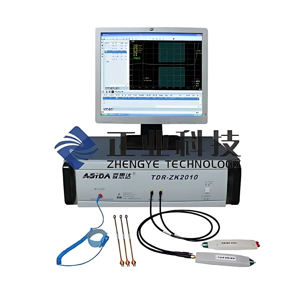
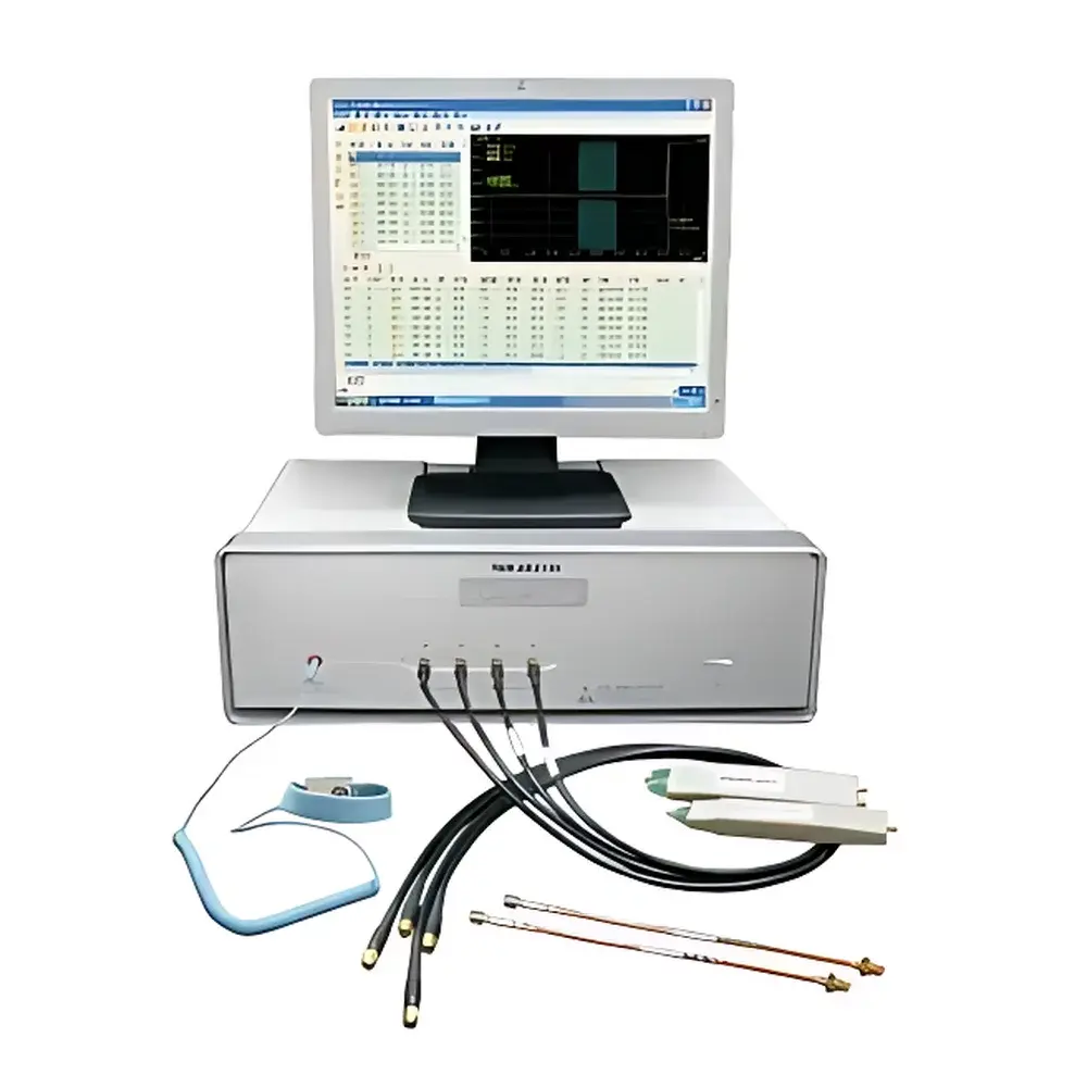
The Oxford Instruments TDRZK2130 is a high-precision time-domain reflectometry (TDR)-based impedance analyzer engineered specifically for printed circuit board (PCB) manufacturing and validation environments. It operates on the fundamental principle of launching a fast-rising step signal into a transmission line (e.g., microstrip, stripline, or differential pair) and analyzing the reflected waveform to extract characteristic impedance profiles along the trace length. Unlike frequency-domain methods, TDR provides spatially resolved impedance mapping with sub-millimeter localization—enabling detection of discontinuities, impedance mismatches, via stubs, solder mask effects, and dielectric inhomogeneities. Designed for integration into R&D labs, design verification centers, and high-volume production QA lines, the TDRZK2130 delivers repeatable, traceable, and standards-aligned measurements critical for high-speed digital, RF, and mixed-signal PCBs operating up to 10 Gbps and beyond.
Key Features
- True dual-channel, quad-channel, and optional 8-channel parallel measurement architecture—enabling simultaneous evaluation of multiple traces or differential pairs without manual re-probing.
- 3 GHz real-time bandwidth ensures accurate resolution of impedance anomalies down to ~50 mm spatial scale (based on signal propagation velocity in FR-4), supporting DDR5, PCIe Gen5, and USB4 interconnect validation.
- Automated calibration routine compliant with IPC-TM-650 Section 2.5.5.7, including open/short/load compensation and reference plane de-embedding for fixture-induced error correction.
- Integrated Windows-based control software with intuitive GUI, drag-and-drop test sequence builder, and configurable pass/fail thresholds per trace segment.
- Real-time waveform overlay, delta-Z deviation mapping, and statistical process control (SPC) charts—including Cp/Cpk calculation—for batch-level impedance consistency monitoring.
- Hardware-accelerated data acquisition engine enabling <500 ms average test cycle time per trace (including auto-triggering, averaging, and report generation).
- Non-contact probe interface compatibility (optional) for inline or conveyor-integrated deployment in automated optical inspection (AOI) or automated optical metrology (AOM) workflows.
Sample Compatibility & Compliance
The TDRZK2130 supports rigid, flex, and rigid-flex PCB substrates with standard copper thicknesses (1/2 oz to 3 oz), common dielectrics (FR-4, Rogers RO4000®, Megtron, Isola I-Tera), and surface finishes (ENIG, immersion silver, OSP). It accommodates trace widths from 50 µm to 500 µm and spacing ≥ 75 µm. All measurement protocols adhere to IPC-TM-650 Method 2.5.5.7 (“Characteristic Impedance of Printed Board Traces Using Time Domain Reflectometry”) and IPC-2141A (“Design Guidelines for High-Speed Controlled Impedance Circuit Boards”). The system’s firmware and data handling architecture support audit-ready operation under GLP and GMP frameworks, with optional 21 CFR Part 11-compliant electronic signatures and full metadata logging (operator ID, timestamp, environmental conditions, calibration status).
Software & Data Management
The embedded TDRControl Suite v4.x provides full lifecycle test management: from template-driven test plan creation (with trace geometry, stack-up definition, and impedance target windows) to automated execution, raw waveform archiving (in IEEE Std 1159-compliant .tdr binary format), and export to CSV, PDF, or XML for MES/SPC integration. All reports include calibrated impedance vs. distance plots, statistical summaries (mean, std dev, min/max, outlier count), and compliance flags against user-defined IPC or internal spec limits. Audit trails record every parameter change, calibration event, and result export—retained for ≥18 months per default configuration. Data encryption (AES-256) and role-based access control (RBAC) are available for regulated environments.
Applications
- Pre-production design validation of high-speed channel topologies (e.g., memory buses, SerDes lanes, RF front-end routing).
- In-process impedance verification during panel fabrication—before drilling, plating, or solder mask application.
- Root-cause analysis of signal integrity failures via impedance discontinuity localization (e.g., connector transitions, split planes, thermal relief patterns).
- Supplier qualification and incoming material verification against controlled impedance specifications.
- Process capability studies across etch, lamination, and surface finish steps to quantify impedance drift and correlation with process parameters.
- Support for advanced packaging substrates (ABF, Ajinomoto Build-up Film) and HDI microvia stacks where traditional TDR fixtures require custom launch solutions.
FAQ
What calibration procedure is required before daily use?
A full 3-point (open-short-load) calibration using the supplied NIST-traceable calibration kit is recommended at system startup and after ambient temperature shifts >3°C. Warm-up time is 30 minutes minimum.
Can the TDRZK2130 measure impedance of embedded passive components or buried traces?
Yes—when used with appropriate high-frequency probe stations and de-embedded launch structures, it resolves impedance of buried layers up to 8-layer stacks, provided the test structure includes dedicated TDR access vias per IPC-2141 Annex B.
Is remote operation and data export supported for factory automation systems?
The instrument features Ethernet (TCP/IP) and USB 3.0 interfaces with SCPI command set compliance. RESTful API and OPC UA adapters are available as licensed options for MES/SCADA integration.
How does the system handle impedance variation caused by solder mask thickness non-uniformity?
The software includes a built-in dielectric overlay compensation module that accepts measured or modeled solder mask Dk/Df values and adjusts the effective relative permittivity profile accordingly—reducing systematic offset by up to 2.3 Ω in typical FR-4 + LPI configurations.
What is the maximum trace length that maintains ±1% accuracy at 150 Ω?
At 150 Ω nominal, the specified accuracy holds for trace lengths ≤1.2 m when using low-loss coaxial launch cables and proper grounding; beyond 1.2 m, attenuation correction algorithms apply based on measured insertion loss per IPC-TM-650 2.5.5.14.


