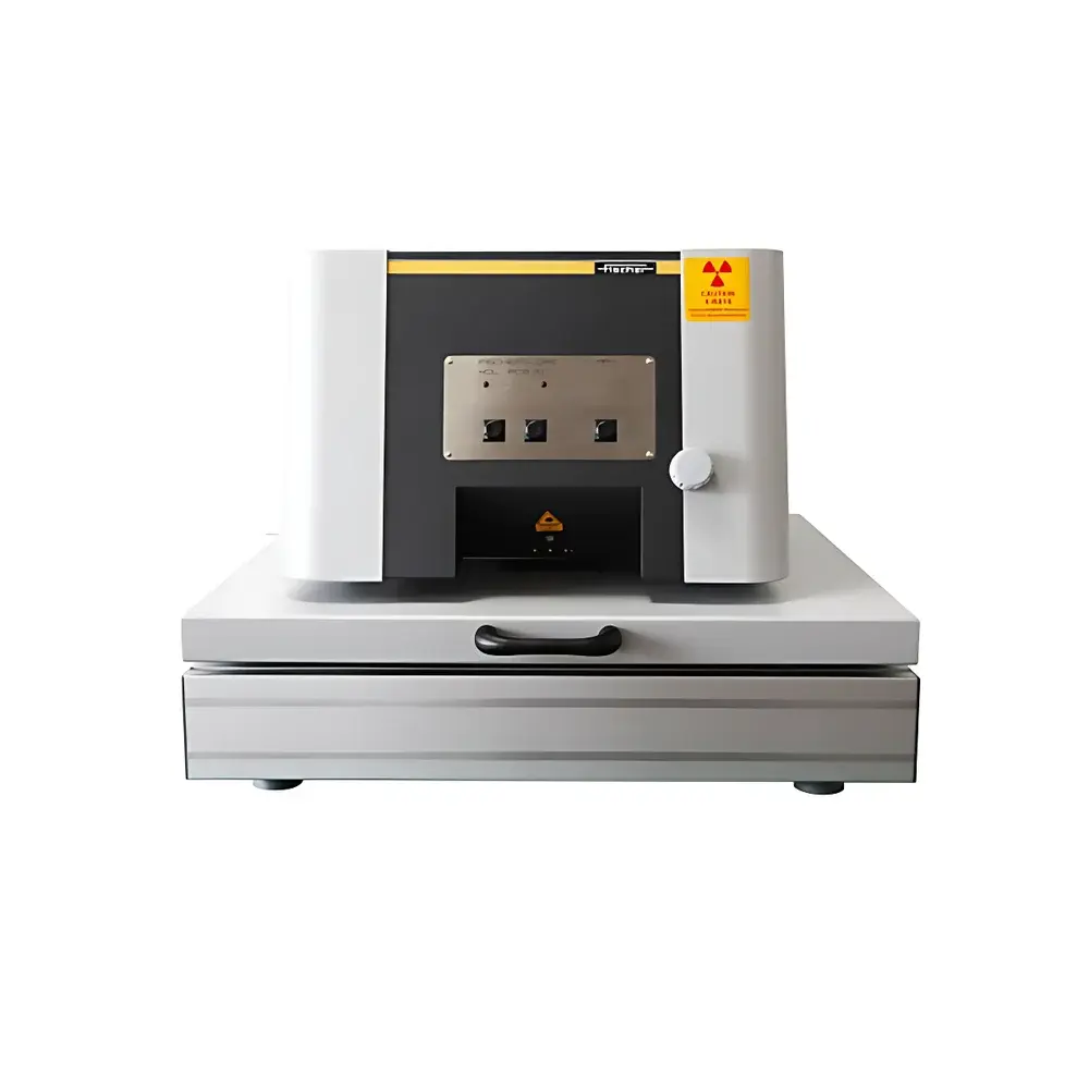
XDLM-PCB Series X-Ray Fluorescence Thickness Analyzer for Multilayer PCB Plating
| Origin | Guangdong, China |
|---|---|
| Manufacturer Type | Authorized Distributor |
| Origin Category | Domestic (China) |
| Model | XDLM-PCB 200 / 210 / 220 |
| Price Range | USD 70,000 – 140,000 |
| Standards Compliance | DIN ISO 3497, ASTM B568 |
| Sample Positioning | Motorized XY Stage (210/220), Manual Drawer-Type Stage (200) |
| Imaging System | High-Resolution Color Camera with Real-Time Overlay |
| Software Platform | WINFTM® v5.2 (Windows-based, CFR Part 11 Ready) |
Overview
The XDLM-PCB Series is a benchtop energy-dispersive X-ray fluorescence (EDXRF) thickness analyzer engineered specifically for non-destructive, quantitative measurement of multi-layer metallic coatings on printed circuit boards (PCBs). Leveraging fundamental parameter (FP)-based quantification and calibrated monochromatic excitation, the system delivers traceable, repeatable thickness data for sequential plating layers—including Cu, Ni, Sn, Au, Pd, Ag, and Pb-free solder—without requiring destructive cross-sectioning or reference standards for routine operation. Designed for QC laboratories in PCB fabrication, EMS providers, and contract manufacturers, the XDLM-PCB platform operates under ambient air conditions and requires no vacuum pumping or helium purging, minimizing operational overhead while maintaining sub-micrometer resolution for thin-film stacks down to 0.05 µm.
Key Features
- Three configuration tiers: XDLM-PCB 200 (manual drawer-stage entry), XDLM-PCB 210 (motorized XY stage with 100 × 100 mm travel, ±1 µm repeatability), and XDLM-PCB 220 (enhanced 200 × 200 mm XY stage with auto-focus camera and Z-axis height compensation)
- Integrated coaxial high-resolution color camera (5 MP, real-time overlay with XRF measurement spot) enabling visual verification of analysis position and layer edge detection
- Laser-assisted sample alignment system (650 nm diode, Class II) co-registered with the X-ray beam path for rapid initial positioning
- Optimized low-power X-ray tube (50 kV, 1 mA max) with selectable anodes (Rh, Mo, W) and primary beam filters to enhance peak-to-background ratio for light-element sensitivity (e.g., P, S in ENIG)
- Si-PIN or SDD detector options (depending on model), offering energy resolution ≤145 eV at Mn Kα for robust spectral deconvolution of overlapping lines (e.g., Ni Kβ / Cu Kα)
- Pre-installed WINFTM® v5.2 software with embedded calibration libraries for common PCB plating systems (ENIG, ENEPIG, HASL, OSP, immersion Ag)
Sample Compatibility & Compliance
The XDLM-PCB accommodates standard PCB formats up to 300 × 300 mm (220 model) or 200 × 200 mm (210/200 models), with Z-height clearance of 45 mm to accommodate mounted components or uneven substrates. Sample clamping is tool-free and adjustable via pneumatic or mechanical fixtures (model-dependent). All configurations comply with DIN ISO 3497:2022 (“Metallic coatings — Measurement of coating thickness — X-ray spectrometric methods”) and ASTM B568-19 (“Standard Test Method for Thickness of Metallic Coatings by X-Ray Spectrometry”), supporting audit-ready reporting for ISO 9001, IATF 16949, and IPC-A-600 qualified environments. Instrument firmware and software support GLP/GMP workflows, including electronic signatures, audit trail logging, and user role-based access control per FDA 21 CFR Part 11 requirements.
Software & Data Management
WINFTM® provides a validated, Windows-native interface for method development, batch measurement scheduling, statistical process control (SPC), and report generation. Key capabilities include multi-point mapping (grid or custom coordinate import), layer stack modeling with interdiffusion correction, and automatic detection of plating anomalies (e.g., skip-plating, edge thinning, voids) via intensity variance thresholds. Raw spectra are stored in standardized .SPE format; measurement metadata (operator ID, timestamp, stage coordinates, tube settings) is embedded in XML headers. Data export supports CSV, PDF, and industry-standard XML-DA for integration with MES or LIMS platforms. Software validation documentation (IQ/OQ/PQ templates) and change control logs are provided with each system.
Applications
- Quantitative thickness verification of electroless nickel immersion gold (ENIG) layers: Ni (2–6 µm) + Au (0.05–0.2 µm)
- Thickness and composition analysis of electroless palladium immersion gold (ENEPIG) stacks
- Measurement of lead-free hot-air solder leveling (HASL) SnCu alloy thickness and Cu dissolution depth
- OSP (organic solderability preservative) film thickness estimation via Cu Kα attenuation modeling
- Process validation and incoming inspection of PCB panels prior to assembly
- Failure analysis root-cause correlation between plating non-uniformity and solder joint reliability metrics
FAQ
Does the XDLM-PCB require annual recalibration by the manufacturer?
No—each unit ships with a NIST-traceable calibration certificate and built-in reference check sources. Users perform daily verification using certified reference foils; full recalibration is recommended only after major hardware service or every 12 months per internal QA policy.
Can the system measure through solder mask?
Yes—EDXRF penetration depth in polymer-based solder masks (typically 20–50 µm thick) is sufficient for underlying Cu trace thickness measurement, though accuracy decreases beyond 30 µm mask thickness due to matrix absorption effects.
Is WINFTM® compatible with Windows 11 and 64-bit architectures?
Yes—WINFTM® v5.2 is certified for Windows 10 (64-bit) and Windows 11 (22H2 and later), with driver signing compliant with Microsoft WHQL requirements.
What safety certifications does the instrument hold?
The XDLM-PCB series complies with IEC 61010-1:2010 (Safety Requirements for Electrical Equipment for Measurement, Control, and Laboratory Use) and carries CE marking, RoHS 2011/65/EU, and FCC Part 15 Class B certification.
Can measurement data be exported directly to Excel or SAP QM modules?
Yes—CSV export includes all raw intensities, fitted thicknesses, uncertainties, and metadata. Optional SAP QM connector module enables direct upload of inspection lots via RFC calls, with configurable field mapping to QM-IM header and item structures.
Related Products


")