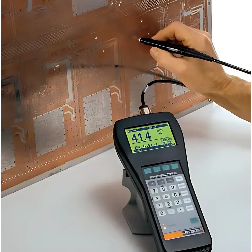
Fischer PMP10 PCB Copper Thickness Gauge
| Origin | Germany |
|---|---|
| Manufacturer Type | Authorized Distributor |
| Origin Category | Imported |
| Model | Fischer PMP10 |
| Pricing | Upon Request |
Overview
The Fischer PMP10 PCB Copper Thickness Gauge is a handheld, non-destructive eddy current-based measurement system engineered for high-precision thickness evaluation of conductive coatings—particularly copper—on non-conductive or ferromagnetic substrates. It operates on the principle of phase-sensitive eddy current testing, where an alternating magnetic field generated by a probe induces eddy currents in the conductive layer; the resulting phase shift and impedance change are quantitatively correlated to coating thickness. Unlike destructive cross-sectioning or X-ray fluorescence (XRF), the PMP10 delivers rapid, repeatable measurements without sample preparation, making it indispensable for in-line quality control in PCB manufacturing, electroplating facilities, and metal finishing labs. Its design adheres to the physical constraints and metrological requirements defined in ISO 2360 (non-magnetic coatings on magnetic substrates) and ASTM B499 (magnetic and eddy current measurement of non-magnetic coatings on magnetic base metals), ensuring traceability and inter-laboratory comparability.
Key Features
- Phase-resolved eddy current technology enabling accurate thickness determination of Cu layers on FR-4, polyimide, and other dielectric substrates—even beneath solder mask.
- Dedicated probe portfolio optimized for specific geometries and material systems: ESD20CuNi/Fe for Cu/Ni on steel; ESD2.4 for small-area Zn coatings on fasteners; ESL080 for through-hole wall copper in multilayer PCBs.
- Multi-frequency capability (60 kHz / 240 kHz) for Ni plating on ferrous substrates—allowing optimal signal-to-noise ratio across thickness ranges from 0.1 µm to 150 µm.
- Compact ergonomic housing with integrated display and intuitive push-button interface—designed for extended use in production environments and cleanroom-adjacent workstations.
- No substrate-specific recalibration required for parts with varying curvature or geometry, thanks to automatic lift-off compensation and built-in probe recognition.
Sample Compatibility & Compliance
The PMP10 supports measurement of conductive layers—including Cu, Ni, Zn, and Al—on both ferromagnetic (e.g., Fe, low-carbon steel) and non-ferromagnetic (e.g., Cu, brass, aluminum) substrates. It is validated for use on printed circuit boards with solder mask, conformal coatings, and silkscreen layers; on electroplated fasteners and automotive components; and on galvanized sheet metal with surface roughness up to Ra 12.5 µm. All probes comply with IEC 61000-4-2 (ESD immunity) and IP54 ingress protection. Measurement uncertainty conforms to ISO/IEC 17025–accredited calibration practices when used with certified reference standards traceable to PTB (Physikalisch-Technische Bundesanstalt).
Software & Data Management
Data acquisition and reporting are managed via Fischer’s FISCHER DataCenter software (v5.2+), supporting bidirectional communication via USB or Bluetooth. The platform enables batch export in CSV, XML, and PDF formats compliant with FDA 21 CFR Part 11 requirements—including electronic signatures, audit trails, and user access controls. Measurement records include timestamp, operator ID, probe serial number, environmental temperature, and raw phase/impedance values. Calibration history, tolerance band configuration, and statistical process control (SPC) charts (X̄/R, Cpk) are fully configurable per test program.
Applications
- Verification of inner-layer and outer-layer copper thickness on rigid and flex PCBs prior to etching and lamination.
- Quantification of copper plating thickness inside drilled through-holes and microvias—critical for current-carrying capacity and thermal reliability assessment.
- In-process monitoring of electroless copper deposition rates in HDI board fabrication lines.
- Quality assurance of zinc and nickel plating on stamped steel components in automotive and aerospace supply chains.
- Post-plating validation of copper cladding on bimetallic busbars and RF shielding enclosures.
FAQ
Can the PMP10 measure copper thickness under solder mask without removal?
Yes—the ESD20CuNi/Fe probe is specifically calibrated for Cu-on-dielectric measurements through typical solder mask thicknesses (20–50 µm) with ±0.3 µm repeatability at 95% confidence.
Is probe calibration required for each new substrate type?
No—phase-sensitive eddy current operation eliminates the need for substrate-specific zeroing; only two-point calibration using certified foil standards is required before daily use.
Does the instrument support GLP/GMP documentation workflows?
Yes—FISCHER DataCenter provides full ALCOA+ compliant data integrity: attributable, legible, contemporaneous, original, accurate, complete, consistent, enduring, and available.
What is the minimum measurable copper thickness on FR-4?
The ESL080 probe achieves reliable detection down to 5 µm Cu on FR-4, with resolution of 0.1 µm in the 5–100 µm range.
Are replacement probes supplied with NIST-traceable calibration certificates?
All Fischer-certified probes ship with individual calibration reports traceable to PTB and include lifetime recalibration service options under contract.
Related Products


")