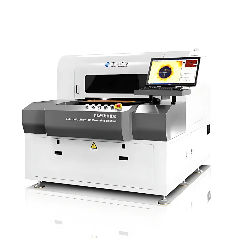
Zhengye XK32 Automated Line Width & Pitch Measurement System
| Brand | Zhengye |
|---|---|
| Model | XK32 |
| Type | Automated Optical Metrology System for PCB, IC, and Flat Panel Display Fabrication |
| Origin | Guangdong, China |
| Manufacturer | Zhengye (OEM/ODM Capable) |
| Dimensions | 1700 mm × 2050 mm × 1600 mm (W×D×H) |
| Weight | ~1750 kg (excl. PC) |
| Power Supply | 3P AC 380 V + N + PE, 50 Hz, 5 kW |
| Operating Temperature | 20–40 °C |
| Relative Humidity | 40–70 % RH |
| Lens | Motorized Zoom Objective (0.7×–4.5×) |
| Field of View (at specified magnifications) | 0.7× = 3.5 mm, 1× = 3.2 mm, 2× = 2.2 mm, 3× = 1.5 mm, 4× = 1.0 mm (±5 % tolerance) |
| Measurement Accuracy (Line Width) | ±1 µm at 3× and 4× magnification |
| Minimum Measurable Line Width | 20 µm |
| Maximum Measurable Line Width | 1200 µm |
| Measurement Range (X–Y) | ≤600 mm × 650 mm |
| Illumination | High-Stability LED Ring Light |
| Edge Detection | Auto-Thresholding + Sub-Pixel Interpolation Algorithm |
| Navigation | CCD-Based Macro-Micro Hybrid Imaging with Real-Time Coordinate Mapping |
| Software Interface | Windows-based GUI with DXF Import, Program Scripting, Statistical Reporting, and Excel Export (CSV/XLSX) |
| Compliance | Designed per ISO 9001 manufacturing practices |
Overview
The Zhengye XK32 Automated Line Width & Pitch Measurement System is a high-precision optical metrology platform engineered for inline and offline dimensional inspection in advanced microfabrication environments. It operates on the principle of digital image acquisition combined with sub-pixel edge detection algorithms, enabling non-contact, high-reproducibility measurement of critical geometric features—including line width, line-to-line pitch, hole-to-edge distance, circular/oval aperture diameters, and blind via dimensions. Primarily deployed in printed circuit board (PCB) manufacturing—specifically after etching (pre-solder mask application)—the system also serves semiconductor wafer-level packaging, IC substrate production, and flat-panel display (LCD/OLED) panel fabrication where trace geometry fidelity directly impacts electrical performance and yield. Its modular architecture integrates motorized zoom optics, programmable illumination, and coordinate-mapped navigation to support both R&D validation and high-volume production floor deployment.
Key Features
- DXF-driven automated measurement programming: Users import design files (DXF/DWG), define custom measurement points (e.g., target traces, vias, fiducials), and generate repeatable inspection routines without manual point-and-click operation.
- Motorized continuous zoom lens (0.7×–4.5×) with software-controlled magnification switching—eliminating mechanical lens exchange and enabling dynamic FOV adaptation during single-run multi-scale inspections.
- Auto-focus algorithm synchronized with stage motion ensures consistent focus depth across large-area substrates (up to 600 mm × 650 mm), critical for maintaining measurement integrity on warped or uneven panels.
- Hybrid navigation system: A macro-level CCD camera provides real-time wide-field overview and rapid coarse positioning; the high-resolution measurement camera then engages for micron-level feature localization and quantification.
- Adaptive edge detection engine supports both automatic threshold-based segmentation and manual override—enabling robust line extraction under variable contrast, surface oxidation, or residual resist conditions.
- Comprehensive statistical process control (SPC) toolkit: Built-in capability to compute Cp/Cpk, X-bar & R charts, histogram distribution, and outlier flagging—all exportable in native Excel-compatible formats (XLSX/CSV) with full metadata (timestamp, operator ID, program name, machine ID).
Sample Compatibility & Compliance
The XK32 accommodates rigid and semi-flexible substrates up to 650 mm in length and 600 mm in width, including FR-4, polyimide, ceramic, silicon wafers (up to 12-inch equivalent), and glass TFT-LCD panels. Its optical path and illumination design minimize glare and shadow artifacts on reflective or matte-finished surfaces. While not certified to ISO/IEC 17025 as a calibration laboratory instrument, the system is manufactured under ISO 9001:2015 quality management systems. Its data logging architecture—featuring immutable timestamps, user authentication, and versioned measurement scripts—supports alignment with GLP (Good Laboratory Practice) and internal GMP documentation requirements. Traceability to NIST-traceable standards is achievable via customer-supplied reference artifacts (e.g., NIST SRM 2051 line-width standards).
Software & Data Management
The proprietary Windows-based control software includes a dual-mode interface: engineering mode (for program development, parameter tuning, and algorithm validation) and production mode (locked-down for operator use with role-based access control). All measurement programs are saved as encrypted XML files containing coordinate sets, magnification profiles, exposure settings, and pass/fail thresholds. Audit logs record every action—including login/logout events, program execution, parameter changes, and data export—with SHA-256 hashing for integrity verification. Raw images and processed edge maps are stored alongside numerical results, supporting root-cause analysis during FA (failure analysis) investigations. Integration with MES/SPC platforms is enabled via TCP/IP API and configurable OPC UA server modules (optional add-on).
Applications
- PCB: Quantitative verification of etch uniformity—measuring top/bottom line widths, taper angle estimation, isolation gap consistency, and registration accuracy relative to drill holes or solder mask openings.
- Semiconductor Packaging: Critical dimension (CD) monitoring of redistribution layers (RDL), bump pads, and fine-pitch copper traces on fan-out wafer-level packages (FOWLP).
- Display Manufacturing: Line width and spacing validation on TFT array substrates, touch sensor metal grids (ITO/Cu mesh), and color filter black matrix patterns.
- Advanced Substrates: Dimensional stability assessment of embedded passive components, laser-drilled microvias, and plating thickness correlation (via cross-sectional correlation studies).
- Process Development: Rapid feedback loop for dry/wet etch chemistry optimization, photoresist selection, and exposure dose calibration.
FAQ
What is the minimum measurable line width, and under what conditions is the ±1 µm accuracy guaranteed?
The system resolves features down to 20 µm with standard configuration. The ±1 µm line width accuracy specification applies when operating at 3× or 4× magnification using a calibrated reference standard (e.g., Zhengye-certified quartz scale or NIST SRM 2051), under controlled environmental conditions (23 ± 2 °C, <60 % RH), and with optimal lighting contrast.
Does the system support integration with factory automation protocols (e.g., SECS/GEM, OPC UA)?
Yes—OPC UA server functionality is available as an optional software module. SECS/GEM integration requires custom driver development, supported under Zhengye’s OEM engineering services agreement.
Can measurement programs be transferred between multiple XK32 units?
Yes—programs are hardware-agnostic and portable across identical XK32 configurations. Cross-unit validation is recommended following installation due to minor mechanical tolerances in stage positioning and lens calibration.
Is remote diagnostics or software update capability included?
Remote desktop-assisted troubleshooting is supported via secure TLS-encrypted channel. Over-the-air firmware updates are not enabled by default but can be provisioned under signed maintenance contract with pre-deployment validation.
What documentation is provided for regulatory compliance in medical or aerospace PCB production?
A comprehensive IQ/OQ documentation package—including installation checklist, operational test protocols, calibration certificate templates, and SPC validation reports—is available upon request and aligns with FDA 21 CFR Part 11 electronic record requirements when deployed with optional audit trail and e-signature modules.
")


