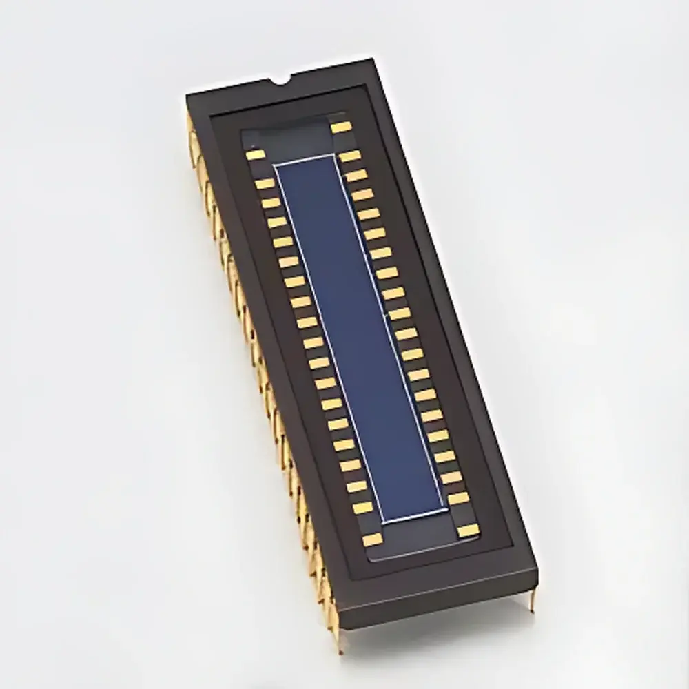
Hamamatsu S4111-35Q Silicon Photodiode Array
| Brand | Hamamatsu |
|---|---|
| Origin | Japan |
| Manufacturer Type | Original Equipment Manufacturer (OEM) |
| Product Category | Imported Optical Component |
| Model | S4111-35Q |
| Element Size (per column) | 4.4 × 0.9 mm |
| Number of Elements | 35 |
| Package | Ceramic 40-pin DIP |
| Cooling Method | Non-cooled |
| Maximum Reverse Voltage | 15 V |
| Spectral Response Range | 190–1100 nm |
| Peak Responsivity Wavelength (typ.) | 960 nm |
| Responsivity (typ.) | 0.58 A/W at 960 nm |
| Dark Current (max.) | 10 pA per element at VR = 10 mV |
| Rise Time (typ.) | 1.2 μs at VR = 0 V |
| Junction Capacitance (typ.) | 550 pF at VR = 0 V |
| Operating Temperature | Typical Ta = 25 °C |
Overview
The Hamamatsu S4111-35Q is a linear silicon photodiode array engineered for high-fidelity spectral detection across the ultraviolet-to-near-infrared (UV–NIR) range (190–1100 nm). Housed in a hermetically sealed ceramic dual-in-line package (40-pin DIP), this 35-element monolithic array leverages optimized silicon junction design to deliver stable, low-noise performance in demanding optical instrumentation environments—including UV-Vis-NIR spectrophotometers, process analytical technology (PAT) systems, and benchtop spectroscopic sensors. Unlike CCD or CMOS-based detectors, the S4111-35Q operates in photovoltaic or reverse-biased mode, enabling charge-integration readout with minimal thermal drift and no clock-induced charge (CIC) artifacts. Its wide spectral coverage, combined with peak responsivity at 960 nm (0.58 A/W), makes it particularly suitable for applications requiring sensitivity in the NIR region where many organic compounds exhibit characteristic absorption bands.
Key Features
- UV–NIR Broadband Sensitivity: Uniform quantum efficiency from 190 nm (deep UV) to 1100 nm (near-infrared), supported by quartz or fused-silica window options—enabling compatibility with deuterium, tungsten-halogen, and LED-based light sources.
- Low Crosstalk Architecture: Optimized inter-element isolation reduces optical and electrical crosstalk, preserving spatial resolution and signal fidelity during multi-channel spectral acquisition.
- Low Dark Current Performance: Maximum dark current of 10 pA per element (at VR = 10 mV) ensures high signal-to-noise ratio (SNR) in low-light applications such as absorbance measurements below 0.01 AU.
- Large Active Area per Element: Each 4.4 × 0.9 mm photosensitive segment provides enhanced photon collection efficiency without requiring external focusing optics—reducing system complexity and alignment sensitivity.
- Robust Ceramic Packaging: Hermetic ceramic DIP construction ensures long-term reliability under variable humidity and thermal cycling conditions typical in industrial QA/QC labs and field-deployable analyzers.
- Flexible Biasing & Readout: Supports both zero-bias (photovoltaic) and reverse-biased operation up to 15 V, allowing trade-offs between speed (lower junction capacitance at higher bias) and linearity (reduced leakage effects).
Sample Compatibility & Compliance
The S4111-35Q is designed for integration into optical paths compliant with ISO/IEC 17025-accredited measurement systems. Its spectral response aligns with ASTM E308 (Standard Practice for Computing the Colors of Objects) and supports traceable radiometric calibration when paired with NIST-traceable reference lamps. The device meets RoHS Directive 2011/65/EU requirements and is compatible with standard surface-mount and through-hole PCB assembly processes. As a bare detector component—not a complete instrument—it falls outside FDA 21 CFR Part 11 scope; however, when embedded in validated analytical instruments (e.g., pharmaceutical dissolution testers or environmental water quality analyzers), its stable responsivity enables GLP/GMP-compliant data generation with full audit trail support via host-system firmware.
Software & Data Management
While the S4111-35Q itself is an analog front-end component, it interfaces seamlessly with industry-standard analog-to-digital conversion architectures—including 16-bit or higher simultaneous-sampling ADCs (e.g., Texas Instruments ADS8860 series) and FPGA-based timing controllers. Hamamatsu provides detailed application notes (e.g., “Driving and Reading Linear Photodiode Arrays”) covering optimal biasing networks, noise-reduction layout guidelines, and correlated double sampling (CDS) techniques to suppress reset noise and 1/f flicker. Integration with LabVIEW™, MATLAB® Data Acquisition Toolbox, or Python-based frameworks (e.g., PyVISA + NumPy) is straightforward using programmable gain instrumentation amplifiers and multiplexed sample-and-hold circuits. Raw output data retains full linearity over ≥99.8% of full scale, facilitating post-acquisition correction for pixel-to-pixel responsivity nonuniformity using factory-measured gain maps (available upon request).
Applications
- UV-Vis-NIR spectrophotometers for pharmaceutical raw material identification (per USP and EP 2.2.25)
- In-line monitoring of chemical reaction kinetics in flow cells and microfluidic platforms
- Portable gas analyzers utilizing differential optical absorption spectroscopy (DOAS)
- Calibration transfer standards in metrology laboratories supporting ISO/IEC 17025 accreditation
- Multi-wavelength reflectance sensors for agricultural product grading (e.g., grain moisture, fruit sugar content)
- Low-cost OEM spectral engines for educational and industrial teaching platforms
FAQ
What is the recommended reverse bias voltage for optimal SNR in low-light conditions?
For most spectrophotometric applications, a reverse bias of 5–10 V balances dark current suppression with junction capacitance minimization—ensuring rise time remains below 1.5 μs while maintaining linearity within ±0.2% F.S.
Can the S4111-35Q be used without cooling in ambient laboratory environments?
Yes. Its non-cooled design is qualified for continuous operation at Ta = 15–35 °C. For extended integrations (>1 s) at elevated temperatures, dark current compensation algorithms are advised.
Is custom window filtering available directly from Hamamatsu?
Hamamatsu offers optional interference filters (e.g., bandpass, edge, or notch types) mounted on the ceramic package; specifications must be submitted via formal OEM inquiry with optical density and angle-of-incidence requirements.
How does the 40-pin DIP footprint simplify PCB integration?
The standardized 0.1-inch pin pitch and through-hole layout allow direct compatibility with prototyping breadboards, automated pick-and-place assembly, and legacy test fixtures—eliminating the need for adapter boards or reflow-compatible carriers.
What documentation is provided with the component for regulatory validation?
Each batch includes a Certificate of Conformance (CoC) listing measured dark current, responsivity at 960 nm, and spectral uniformity data. Full traceability to Hamamatsu’s internal calibration lab is available upon request for GxP-regulated deployments.


