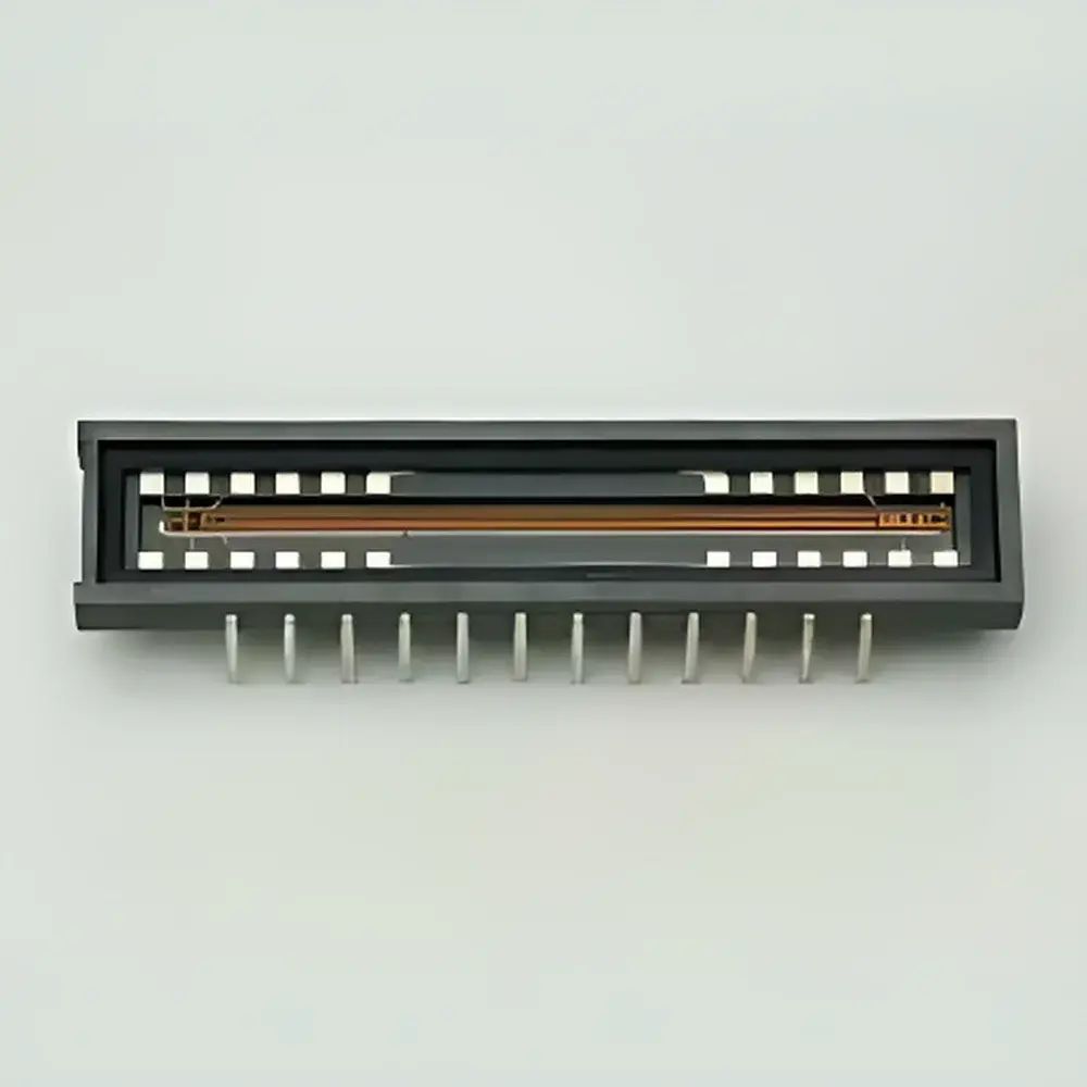
Hamamatsu S1 Series CMOS Linear and Area Image Sensors
| Brand | Hamamatsu |
|---|---|
| Origin | Japan |
| Manufacturer Type | Original Equipment Manufacturer (OEM) |
| Import Status | Imported |
| Component Category | Optical Component |
| Sensor Architecture | CMOS Linear Array & Area Array |
| Package Types | Ceramic, Plastic, and Hermetic Options |
| Key Models | S11639, S12706, S11106, S11107, S8377-Q series, S8378-Q series, S10123-Q series, S10124-Q series, S10227-10, S11106-10, S11107-10, S11662 |
Overview
The Hamamatsu S1 Series comprises high-performance CMOS linear and area image sensors engineered for precision optical measurement, spectral analysis, industrial inspection, and scientific instrumentation. Unlike CCD-based alternatives, these sensors integrate on-chip timing control circuits and analog signal processing amplifiers—enabling operation from a single power supply and simplified external drive logic. This architecture reduces system-level complexity, improves power efficiency, and enhances timing synchronization fidelity—critical for high-speed line-scan applications such as Raman spectroscopy, laser-induced breakdown spectroscopy (LIBS), optical coherence tomography (OCT) beam profiling, and real-time web inspection systems. The S1 family includes both linear (1D) and area (2D) configurations, with pixel geometries optimized for specific optical throughput, spatial resolution, and dynamic range requirements across UV–NIR (200–1100 nm) spectral bands.
Key Features
- Monolithic CMOS integration of pixel array, timing generator, correlated double sampling (CDS), and programmable gain amplifier (PGA)
- Single-supply operation (typically +3.3 V or +5 V DC), minimizing external component count and PCB footprint
- Multiple package options: ceramic LCC (hermetic), plastic DIP, and surface-mount QFN variants for thermal stability and EMI resilience
- Configurable integration time (in select models, e.g., S10123/S10124 series), enabling adaptive exposure control under varying illumination conditions
- High quantum efficiency (>60% at 550 nm for standard silicon variants) and low read noise (<10 e⁻ RMS typical)
- Pixel pitch ranging from 7 µm to 250 µm; active area widths from 6.4 mm to 28.672 mm; lengths up to 2.5 mm for specialized wide-field sensing
- Line rates up to 111,111 lines/s (S11107-10) and frame rates up to 120 fps (S11662 area sensor, full resolution)
Sample Compatibility & Compliance
The S1 Series is designed for integration into OEM optical subsystems requiring traceable metrological performance. Sensors comply with JEDEC J-STD-020 moisture sensitivity level (MSL) standards and are qualified per AEC-Q200 for extended temperature operation (–40 °C to +85 °C ambient). While not certified as standalone medical or safety-critical devices, their electrical and optical characteristics support design-in compliance with ISO/IEC 17025-accredited calibration workflows and GLP/GMP-aligned instrument qualification protocols. For regulated environments (e.g., pharmaceutical process analytical technology), users must validate sensor performance within the final system context per ICH Q2(R2) and FDA 21 CFR Part 11 data integrity requirements.
Software & Data Management
Hamamatsu provides the Lighting Software Development Kit (SDK) for Windows/Linux, supporting direct register-level configuration, real-time streaming acquisition, and hardware-triggered synchronization via TTL/CMOS-compatible input pins. SDK features include dark current subtraction, non-uniformity correction (NUC) tables, ROI selection, and timestamped metadata embedding. Raw output is delivered in 12-bit or 16-bit linear format (configurable), compatible with HDF5, TIFF, and binary formats for downstream analysis in MATLAB, Python (NumPy/SciPy), LabVIEW, or custom C++ pipelines. Audit trails for acquisition parameters—including integration time, gain setting, and clock frequency—are programmatically accessible and exportable to meet ALCOA+ data integrity principles.
Applications
- Spectroscopy: Compact grating spectrometers (UV-VIS-NIR), portable LIBS analyzers, and fluorescence lifetime imaging systems
- Industrial Metrology: High-speed web inspection (paper, film, foil), automated defect detection, and dimensional gauging using triangulation or shadow moiré
- Biomedical Instrumentation: Flow cytometry signal capture, microplate reader detectors, and endoscopic OCT probe receivers
- Laser Diagnostics: Beam profile monitoring (M² measurement), pulse shape analysis, and cavity alignment feedback
- Scientific Research: Time-resolved photoluminescence, pump-probe experiments, and particle image velocimetry (PIV) with sub-microsecond gating
FAQ
What is the difference between linear and area CMOS sensors in the S1 Series?
Linear sensors (e.g., S11639, S12706) provide one-dimensional pixel arrays optimized for scanning applications where motion or dispersion provides the second spatial dimension. Area sensors (e.g., S11662) deliver two-dimensional imaging without mechanical scanning, suitable for snapshot capture and static field-of-view applications.
Do these sensors require external cooling for low-noise operation?
Most S1 models operate effectively at ambient temperatures; thermoelectric cooling is optional and application-dependent. For ultra-low dark current (<0.1 e⁻/pixel/s), Peltier-stabilized mounting is recommended—particularly for long-integration spectroscopic measurements.
Can the S1 sensors be used in vacuum or high-humidity environments?
Ceramic-packaged variants (e.g., S11662, S11639) are rated for moderate vacuum (10⁻³ mbar) and conformally coated versions support IP54-equivalent humidity resistance. Plastic packages are limited to controlled laboratory environments.
Is radiation tolerance specified for space or nuclear applications?
Hamamatsu does not publish total ionizing dose (TID) or single-event effect (SEE) data for standard S1 parts. Radiation-hardened derivatives are available under custom qualification programs upon request.
How is pixel non-uniformity corrected in production systems?
Factory-measured offset/gain maps are provided in calibration files. The SDK supports real-time NUC application during acquisition, with user-updatable tables for drift compensation over time and temperature.


