Hamamatsu MiNY® PL Micro LED Photoluminescence Inspection System C15740-01
| Brand | Hamamatsu |
|---|---|
| Origin | Japan |
| Manufacturer | Hamamatsu Photonics K.K. |
| Type | Imported |
| Model | C15740-01 |
| Wafer Sizes Supported | 100 mm (4″) or 150 mm (6″) |
| Measurement Time | ~12 min (4″ wafer, 10× objective, PL mode) |
| PL Wavelength Range | R/G/B channels |
| Spatial Resolution | 1 µm/pixel (standard), 0.5 µm/pixel (high-res mode) |
| Measured Parameters | Shape defects, PL intensity distribution, PL peak wavelength mapping |
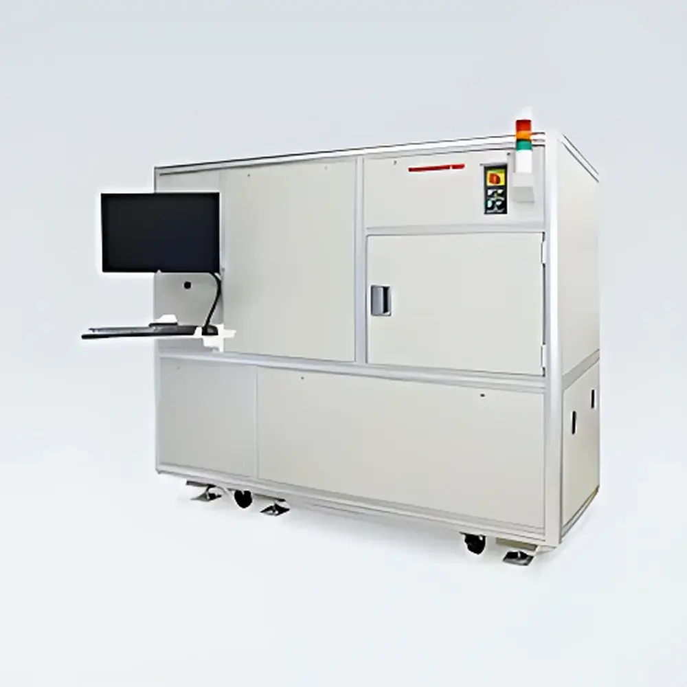
| Dimensions | 2000 mm (W) × 1878 mm (H) × 1130 mm (D) |
| Weight | ~1800 kg |
Overview
The Hamamatsu MiNY® PL Micro LED Photoluminescence Inspection System C15740-01 is a purpose-built, high-precision metrology platform engineered for non-contact, quantitative photoluminescence (PL) characterization of micro-LED arrays on semiconductor wafers. Operating on the principle of excitation-emission spectroscopy, the system employs a stabilized UV or near-UV laser source to uniformly illuminate micro-LED pixel structures, followed by high-sensitivity spectral imaging to capture spatially resolved PL intensity and peak wavelength data across the entire wafer surface. Unlike contact-based electrical testing, PL inspection enables rapid, damage-free assessment of material quality, epitaxial uniformity, quantum well integrity, and pixel-level spectral consistency—critical parameters in the mass production of RGB micro-LED displays, AR/VR microdisplays, and high-brightness micro-optoelectronic devices. Designed for integration into Class 1–100 cleanroom environments, the C15740-01 meets stringent mechanical stability, particulate control, and ESD-safe operational requirements typical of front-end semiconductor fabrication facilities.
Key Features
- Automated wafer handling with vacuum chucking and precision X-Y-Z-θ alignment for repeatable positioning of 100 mm (4″) and 150 mm (6″) wafers; custom configurations available for alternative diameters upon request.
- Dual-resolution optical imaging path: standard mode delivers 1 µm/pixel spatial sampling for throughput-optimized full-wafer screening; high-resolution mode achieves 0.5 µm/pixel for defect root-cause analysis at sub-pixel scale.
- Multi-channel spectral detection architecture enabling simultaneous acquisition of red, green, and blue PL emission bands—supporting quantitative chromaticity mapping and binning compliance verification per display industry standards (e.g., VESA DisplayHDR, JEDEC JESD22-A108).
- Integrated calibration traceability: factory-aligned using NIST-traceable reference standards for radiometric intensity and spectral wavelength accuracy; supports user-performed daily verification via onboard LED reference sources.
- Rigid granite base and active vibration isolation minimize thermal drift and mechanical perturbation, ensuring measurement reproducibility better than ±0.5 nm in peak wavelength and ±2% in integrated PL intensity over 8-hour shifts.
Sample Compatibility & Compliance
The C15740-01 accommodates bare and processed GaN-on-sapphire, GaN-on-Si, and InGaN-based micro-LED wafers with standard backgrinding, passivation, and metal contact layers. It supports both planar and mesa-etched architectures and is compatible with temporary bonding carriers used in hybrid bonding processes. The system conforms to SEMI S2-0201 (safety), SEMI S8-0701 (ergonomics), and ISO 14644-1 Class 5 (ISO Class 5 / Fed Std 209E Class 100) cleanroom compatibility specifications. All internal optics, motion stages, and detector housings are constructed from low-outgassing, non-magnetic stainless steel and anodized aluminum alloys compliant with SEMI F22-0302 material purity guidelines.
Software & Data Management
Controlled via Hamamatsu’s proprietary MiNY PL Studio software suite, the system provides full audit trail functionality aligned with FDA 21 CFR Part 11 requirements—including electronic signatures, role-based access control, and immutable record retention. Data outputs include TIFF-based hyperspectral cubes (intensity + wavelength per pixel), CSV-formatted defect logs with XY coordinates and classification tags (e.g., “shape anomaly”, “intensity dropout”, “wavelength shift > ±3 nm”), and PDF reports compliant with internal quality management systems (QMS) and external customer PPAP submissions. Raw data is stored in HDF5 format for interoperability with MATLAB, Python (NumPy/Hyperspy), and industry-standard statistical process control (SPC) platforms such as JMP or Minitab.
Applications
- Pre-bonding wafer-level screening for micro-LED yield enhancement and process window qualification.
- Root-cause analysis of wavelength non-uniformity linked to MOCVD growth variations or etch-induced strain.
- Verification of color filter alignment and pixel-to-pixel spectral crosstalk in hybrid RGB micro-LED assemblies.
- Qualification of repair outcomes following laser-induced thermal annealing or localized current injection treatments.
- Supporting technology transfer from R&D to high-volume manufacturing through standardized measurement protocols aligned with JEDEC JEP184 and IEC 62795.
FAQ
Is the C15740-01 compatible with automated material handling systems (AMHS)?
Yes—the system features SECS/GEM interface compliance and includes configurable digital I/O ports for integration with factory host systems and overhead hoist transports.
Can PL measurements be correlated with electroluminescence (EL) test data?
While PL and EL probe different physical mechanisms (radiative recombination under optical vs. electrical excitation), Hamamatsu provides cross-modal calibration templates and co-registration tools to enable statistical correlation analysis between PL spectral maps and functional EL test results.
What maintenance intervals are recommended for long-term measurement stability?
Optical alignment verification is recommended quarterly; laser source output power and spectrometer wavelength calibration require semiannual validation using certified reference materials supplied by Hamamatsu.
Does the system support real-time feedback to process tools?
Via optional OPC UA server module, the system can publish aggregated metrics (e.g., mean wavelength deviation, pixel defect density) to MES or APC systems for closed-loop process adjustment.


