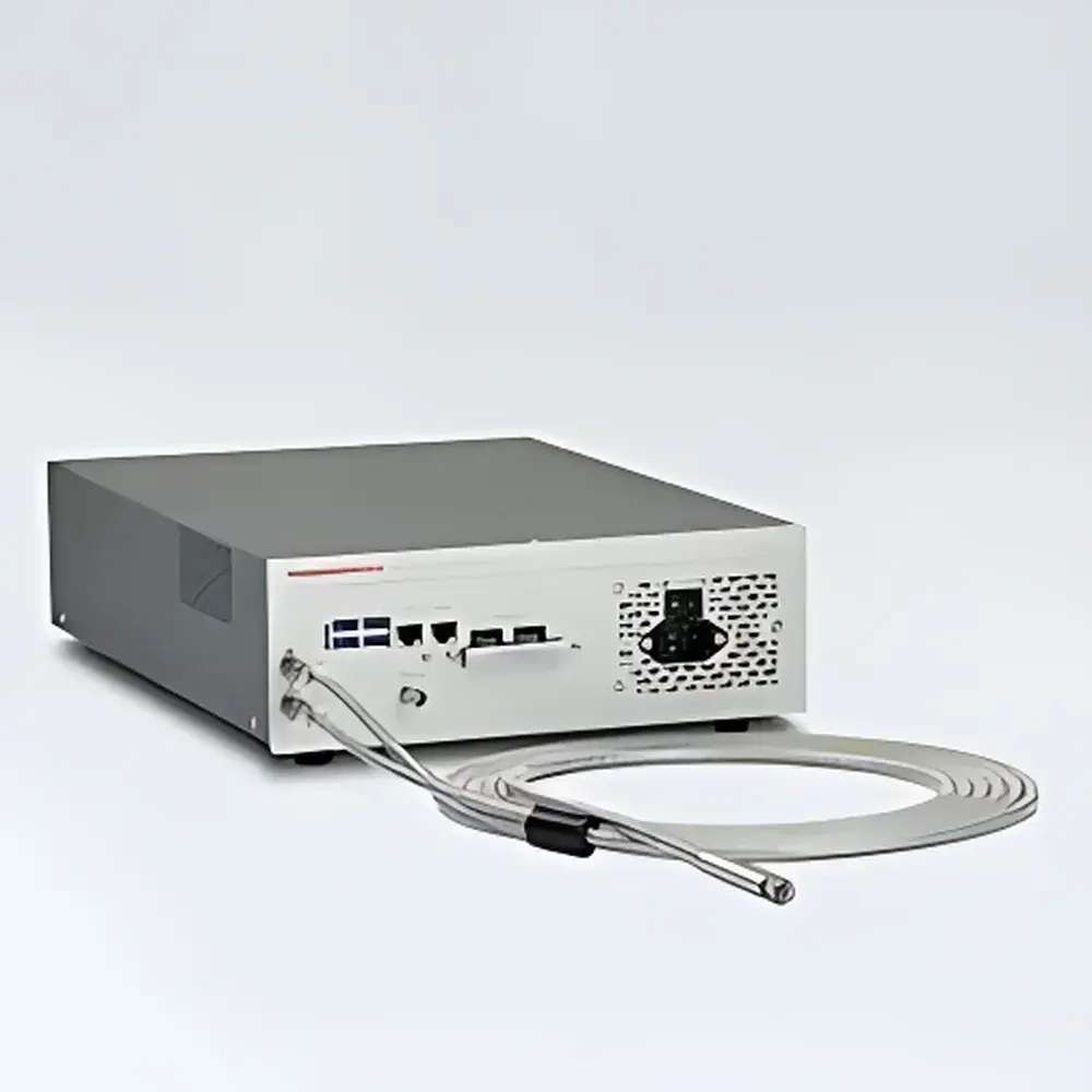
Hamamatsu Optical NanoGauge Thin-Film Thickness Measurement System C12562-04
| Brand | Hamamatsu |
|---|---|
| Origin | Japan |
| Manufacturer | Hamamatsu Photonics K.K. |
| Type | Imported |
| Model | C12562-04 |
| Measurable Thickness Range (on glass substrate, n=1.5) | 500 nm – 300 µm |
| Measurement Repeatability (1 µm glass film) | ±0.2 nm |
| Measurement Accuracy | ±0.4% (per VLSI Standard Measurement Assurance Documentation) |
| Light Source | Halogen lamp |
| Spot Size | ~φ1 mm |
| Working Distance | 10 mm |
| Maximum Layers Analyzable | 10 |
| Analysis Modes | FFT, Curve Fitting, Optical Constant (n, k) Extraction |
| Measurement Speed | Up to 100 Hz (3 ms/point) |
| External Trigger Support | Enhanced TTL-compatible input |
| Interface | RS-232C, Ethernet |
| Power Supply | AC 100–240 V, 50/60 Hz |
| Power Consumption | ~80 VA |
| Fiber Connector | FC |
Overview
The Hamamatsu Optical NanoGauge Thin-Film Thickness Measurement System C12562-04 is an engineered solution for non-contact, real-time optical thickness metrology in semiconductor process control and advanced thin-film manufacturing environments. Based on spectral reflectance interferometry, the system captures high-resolution interference spectra generated at interfaces between layers with differing refractive indices. By applying rigorous Fresnel-based modeling and inverse optical simulation algorithms, it quantifies physical thicknesses and extracts complex refractive index values (n and k) across multilayer stacks — up to ten discrete layers — without requiring physical contact or vacuum conditions. Its design targets critical applications where sub-nanometer repeatability and traceable accuracy are mandated by process node scaling: through-silicon via (TSV) depth monitoring, low-k dielectric film uniformity assessment, adhesive layer characterization in 3D IC packaging, and ultra-thin barrier coating verification on flexible substrates. With a calibrated measurement range spanning 500 nm to 300 µm on standard glass (n = 1.5), the C12562-04 bridges the gap between conventional ellipsometers and mechanical profilometers, delivering high-speed, in-line compatible metrology directly within tool-integrated configurations.
Key Features
- Wide dynamic thickness range: 500 nm – 300 µm on transparent substrates, enabling single-instrument coverage from atomic-layer-deposited (ALD) films to thick polymer encapsulants
- High-speed acquisition: Up to 100 Hz point measurement rate (3 ms per data point), synchronized via programmable external TTL trigger for integration into moving-stage or conveyor-based production lines
- Sub-nanometer repeatability: ±0.2 nm standard deviation on 1 µm reference glass films, validated under controlled environmental conditions per internal calibration protocol
- Multi-layer optical modeling engine: Supports simultaneous fitting of thickness, roughness, and complex refractive index (n + ik) parameters for up to 10-layer stacks using Levenberg-Marquardt optimization
- Modular optical head: Compact φ1 mm spot size and fixed 10 mm working distance facilitate OEM integration into cluster tools, cleanroom-compatible process chambers, or benchtop metrology stations
- Dual-interface control: Native support for RS-232C serial command set and TCP/IP Ethernet communication, enabling seamless integration with SECS/GEM-compliant factory automation systems
Sample Compatibility & Compliance
The C12562-04 is optimized for planar and mildly topographic samples including silicon wafers (bare, oxidized, nitrided), fused silica, sapphire, quartz, and polymer-coated substrates. It accommodates both single-layer films (e.g., SiO₂, SiNₓ, TiN, ITO) and complex stacks (e.g., Cu/Ta/TaOₓ/SiO₂ on Si). Measurement uncertainty is traceably linked to NIST-traceable reference standards and conforms to ASTM E1938-21 (Standard Practice for Spectral Reflectance-Based Thickness Measurement of Transparent Films) and ISO 15632:2017 (Optics and photonics — Interferometric measurement of thin films). For regulated environments, audit-ready data logs—including raw spectra, fit residuals, parameter covariance matrices, and operator timestamps—support GLP and GMP compliance when paired with validated software configurations meeting FDA 21 CFR Part 11 requirements for electronic records and signatures.
Software & Data Management
The bundled NanoGauge Control Software provides a deterministic, scriptable interface for measurement setup, real-time visualization, batch analysis, and export of metrology data in HDF5 and CSV formats. It includes preconfigured templates for common semiconductor film sets (e.g., “SiO₂ on Si”, “Low-k on Cu”), customizable pass/fail thresholds with SPC charting (X-bar/R), and full support for measurement sequence scripting via Python API. All analysis results include uncertainty propagation estimates derived from spectral noise floor, fitting convergence criteria, and material dispersion model fidelity. Raw spectral datasets are stored with embedded metadata (wavelength calibration coefficients, illumination intensity profiles, environmental sensor readings), ensuring long-term reproducibility and facilitating retrospective reanalysis as optical models evolve.
Applications
- Process development and monitoring of ALD, PECVD, and sputtered dielectric layers in front-end-of-line (FEOL) and back-end-of-line (BEOL) fabrication
- In-line thickness verification of bonding adhesives and redistribution layers (RDLs) in fan-out wafer-level packaging (FOWLP)
- Quality assurance of anti-reflective coatings (ARCs), hard masks, and etch-stop layers during lithography and etch module qualification
- Characterization of transparent conductive oxides (TCOs) and perovskite absorber layers in photovoltaic R&D
- Thickness mapping across 200 mm and 300 mm wafers using motorized XY stages (optional accessory)
FAQ
What substrates and film materials can be measured with the C12562-04?
The system supports transparent and semi-transparent films on substrates with known or characterizable optical constants, including Si, SiO₂, Si₃N₄, glass, quartz, sapphire, and polymers such as PI and PET. Opaque metal films require underlying transparent layers or specialized modeling approaches.
Is calibration required before each measurement session?
A one-time wavelength and intensity calibration is performed during initial setup; daily verification using certified reference wafers (e.g., NIST SRM 2030) is recommended for production-critical applications.
Can the system operate in a vacuum or inert atmosphere?
The optical head is not rated for vacuum use; however, it may be mounted externally to vacuum chambers via viewport-compatible optical coupling (custom adapter required).
How is measurement traceability maintained for quality audits?
Each measurement log includes instrument ID, firmware version, calibration certificate ID, environmental conditions (temperature/humidity if monitored), and full spectral data — all exportable for third-party review per ISO/IEC 17025 requirements.
Does the system support automated recipe-driven measurements?
Yes — via Ethernet or RS-232C, users can load predefined measurement protocols (spot position, integration time, layer stack model) and initiate sequences programmatically using ASCII command syntax or Python SDK.


