Hamamatsu C12880MA Miniature Spectrometer Module
| Brand | Hamamatsu |
|---|---|
| Origin | Japan |
| Manufacturer Type | Original Equipment Manufacturer (OEM) |
| Product Category | Imported Optical Component |
| Model | C12880MA |
| Component Type | Optical Sensor Module |
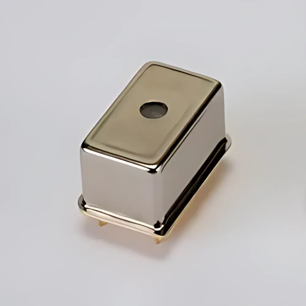
| Dimensions | 20.1 × 12.5 × 10.1 mm |
| Weight | 5 g |
| Spectral Response Range | 340–850 nm |
| Spectral Resolution (FWHM, max) | 15 nm |
| Pixel Count | 256 pixels |
| Operating Temperature | 25 °C (Ta) |
| Enclosure | Hermetically Sealed Package |
| Compliance | RoHS-compliant, JEDEC-standard moisture resistance (MSL 1) |
Overview
The Hamamatsu C12880MA is a miniature, OEM-grade spectrometer module engineered for seamless integration into space-constrained optical systems requiring reliable spectral acquisition across the near-ultraviolet to near-infrared range. Based on a linear CMOS image sensor with integrated slit and fixed grating optics, the device operates on the principle of fixed-grating dispersion coupled with pixel-wavelength mapping—enabling direct intensity-to-wavelength conversion without moving parts. Its compact form factor (20.1 × 12.5 × 10.1 mm, 5 g) and hermetically sealed ceramic package ensure mechanical robustness and long-term stability under variable environmental conditions, particularly in high-humidity settings where conventional open-optic modules risk condensation-induced signal drift or sensor degradation. Designed explicitly for embedded applications—not benchtop analysis—the C12880MA serves as a core photonic sensing element in portable analyzers, industrial process monitors, wearable health sensors, and IoT-enabled spectral endpoints.
Key Features
- Ultra-compact footprint: 20.1 mm (L) × 12.5 mm (W) × 10.1 mm (H), compatible with PCB-level mounting via surface-mount or flex-cable interface
- Hermetic ceramic packaging certified to JEDEC J-STD-020 MSL Level 1, ensuring zero moisture ingress and eliminating need for external desiccation or conformal coating
- Broad spectral response from 340 nm to 850 nm, covering UV-A, visible, and NIR-I bands—ideal for fluorescence excitation monitoring, LED spectral characterization, and colorimetric endpoint detection
- 256-pixel linear CMOS detector with on-chip amplification and correlated double sampling (CDS), delivering high dynamic range (>50 dB) and low read noise (<15 e⁻ RMS)
- Fixed optical path with optimized f-number and slit width, yielding consistent 15 nm FWHM spectral resolution across the full range without calibration drift
- Pre-characterized wavelength calibration coefficients provided per unit in test report (including polynomial coefficients for pixel-to-wavelength mapping)
Sample Compatibility & Compliance
The C12880MA is not a standalone analytical instrument but a calibrated optical sensing module intended for integration into third-party host systems. It accepts collimated or fiber-coupled input (SMA905 or FC/PC optional adapters available separately). No sample preparation is required; compatibility is defined by optical interface geometry and irradiance limits (max. 10 mW/mm² at sensor plane). The module complies with RoHS Directive 2011/65/EU and meets IEC 61000-4-2 (ESD immunity) and IEC 60068-2-30 (damp heat cycling) requirements. While not certified to ISO/IEC 17025 or FDA 21 CFR Part 11, its traceable factory calibration supports GLP-aligned system-level validation when embedded in regulated instrumentation.
Software & Data Management
Hamamatsu provides the C12880MA Evaluation Software (Windows-based) for rapid prototyping, including real-time spectrum visualization, dark current subtraction, and export of ASCII-formatted spectral data (wavelength/intensity pairs). Raw 16-bit digital outputs are accessible via SPI or parallel interface (configurable), enabling deterministic timing control in real-time embedded firmware. For production deployment, developers receive full register maps, timing diagrams, and C-language driver examples compatible with ARM Cortex-M and RISC-V microcontrollers. All calibration metadata—including pixel-specific gain/offset tables and wavelength polynomials—is stored in non-volatile memory on-module and retrievable via command protocol, supporting audit-ready data provenance in regulated environments.
Applications
- Portable blood oximetry and tissue spectroscopy devices leveraging 650–850 nm absorption features
- In-line LED binning and phosphor quality control in semiconductor manufacturing
- UV-curable resin monitoring during additive manufacturing (340–400 nm band)
- Smart agriculture sensors measuring chlorophyll-a/b and carotenoid reflectance indices (500–750 nm)
- Miniaturized environmental monitors for NO₂, O₃, and VOCs using differential optical absorption spectroscopy (DOAS) configurations
- Embedded color matching engines in industrial printing and paint formulation systems
FAQ
Is the C12880MA suitable for quantitative absorbance measurements?
Yes—when paired with a stable broadband source and reference channel, it supports ratiometric absorbance calculation. However, users must implement system-level stray light correction and thermal baseline compensation.
Can it be operated at temperatures outside 25 °C?
The specified performance is guaranteed at Ta = 25 °C. Operation between –10 °C and +60 °C is possible with gain/offset recalibration; Hamamatsu provides temperature-dependent coefficient tables upon request.
Does Hamamatsu offer OEM support for custom firmware or optical modifications?
Yes—custom firmware development, lens/slit redesign, and spectral range tailoring (e.g., UV-enhanced or extended NIR variants) are available under NDA through Hamamatsu’s Industrial Solutions Group.
Is USB connectivity built-in?
No—the module lacks native USB. Interface requires external microcontroller or FPGA with SPI/parallel bus handling; evaluation boards with USB bridge ICs are available separately.
How is spectral calibration traceability maintained across production batches?
Each unit ships with individual calibration certificate referencing NIST-traceable tungsten-halogen and mercury-argon lamp standards; wavelength accuracy is ±1.5 nm across the range, verified per ISO 17025-accredited internal lab procedures.


